В электронной схеме, GND означает Землю, которая определяется как назначенная опорная точка, используемая для измерения напряжений и общий обратный путь для электрических токов. Хотя стандартной практикой является обозначение этого узла как 0 В, GND не обязательно означает физическое заземление земли, защитное заземление или даже отрицательную клемму батареи.
В зависимости от контекста — читаете ли вы схему, подключаете блок питания или разрабатываете печатную плату (PCB) — GND выполняет различные электрические функции. Понимание этих различий необходимо для поддержания целостности сигнала, предотвращения электромагнитных помех (EMI) и обеспечения эксплуатационной безопасности.
30-секундное резюме: Что означает GND?
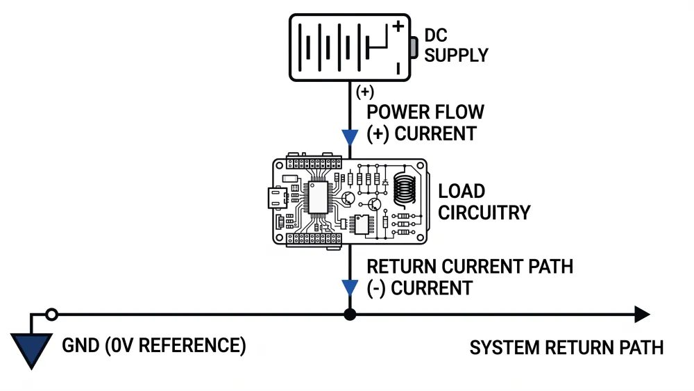
- Опорная точка напряжения: Напряжение всегда измеряется как разность потенциалов между двумя точками. GND — это опорный узел, которому присвоен потенциал 0 В.
- Обратный путь тока: Электрический ток должен образовывать непрерывный контур для протекания. GND обеспечивает путь для возврата тока к его источнику.
- Зависимость от контекста: Заземление схемы может быть плавающим независимо от физической земли (например, в устройстве с батарейным питанием) или может быть напрямую подключено к физическому заземлению земли (PE) для безопасности.
Что означает GND в схеме?
Полная форма GND и практическое определение
В электронике, GND является универсальным сокращением для Землю. Однако рассматривать GND исключительно как физическое соединение с почвой — распространенное заблуждение. В современном проектировании схем GND строго определяется как назначенный опорный узел 0 В в системе.
Поскольку напряжение определяется как разность электрических потенциалов между двумя различными точками, утверждение, что на клемме “+5 В”, просто означает, что ее потенциал на 5 В выше, чем у назначенного узла GND.
Примечание о неэлектронных применениях: Хотя сокращение GND иногда может встречаться в нетехнических контекстах (например, как сокращение для “первый этаж” или “гранд”), в инженерии и физике оно исключительно относится к опорному заземлению схемы или соединению с землей.
Почему “0 В” — это опорная точка, а не магия
Назначение узла как 0 В — это произвольное решение, принятое для удобства измерений. Опорная точка не обладает неотъемлемыми физическими нулевыми энергетическими свойствами и не гарантированно равна абсолютному потенциалу земли.
Рассмотрим три рабочих контекста:
- Плавающие устройства с батарейным питанием: Ручной мультиметр или смартфон работает от батареи. Его внутренний GND является плавающим относительно планеты Земля, однако внутренние цифровые схемы работают корректно относительно этой локальной плоскости 0 В.
- Изолированные DC-DC преобразователи: Промышленные блоки питания часто изолируют входное заземление от выходного заземления с помощью трансформаторов или оптопар. Заземление вторичной стороны электрически развязано от заземления первичной стороны, что позволяет обоим существовать при совершенно разных потенциалах.
- Системы с двухполярным питанием: В схемах операционных усилителей, требующих симметричных шин (например, +15 В и −15 В), GND размещается точно посередине. Здесь GND находится на полпути между самым высоким потенциалом (+15 В) и самым низким потенциалом (−15 В).
| Параметр / Характеристика | Заземление схемы | Заземление земли (PE) | Заземление корпуса | Нейтральный провод (AC) |
|---|---|---|---|---|
| Основное определение | Локальный опорный узел 0 В для сигналов и питания | Физическое соединение с Землей через заземляющие стержни | Металлический корпус или рама оборудования | Токоведущий проводник, соединенный с Землей на главном щите |
| Нормальный ток | Да (переносит обратные токи сигналов/питания) | Нет (переносит ток только при аварийных условиях) | Нет (если не используется намеренно как экран/обратный путь) | Да (замыкает цепь переменного тока обратно на щит) |
| Соединение с Землей | Опционально (может быть плавающим) | Обязательно | Часто подключается к PE для безопасности | Подключено к земле на вводе в здание |
| Основная роль | Установление базового потенциала и цепей обратного тока | Предотвращение поражения электрическим током и отвод тока короткого замыкания | Конструкционная целостность, экранирование и защита от поражения током | Обратный путь для однофазного переменного тока бытовой сети |
Как работает GND? Опорное напряжение и обратный ток
GND задает опорное напряжение
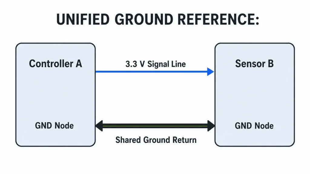
Для точного обмена данными между современными микроконтроллерами, аналого-цифровыми преобразователями (АЦП) и датчиками они должны иметь общий базовый опорный потенциал. Если устройство A передает цифровой сигнал напряжением 3,3 В устройству B, но устройство B не имеет единого опорного узла с устройством A, устройство B не сможет надежно различать логическую единицу (1) и логический ноль (0).
Когда двум изолированным системам необходимо обмениваться данными без общего физического соединения GND, разработчики используют гальванически развязанные интерфейсы, такие как оптопары, цифровые изоляторы или дифференциальные линии связи (например, RS-485 или CAN-шина), для надежного преодоления разрыва в соединении.
Ток должен образовывать замкнутый контур
Электрический ток не исчезает в символе GND на принципиальной схеме; он должен вернуться к своему первоначальному источнику питания. Цепь неполна без замкнутого пути возврата.
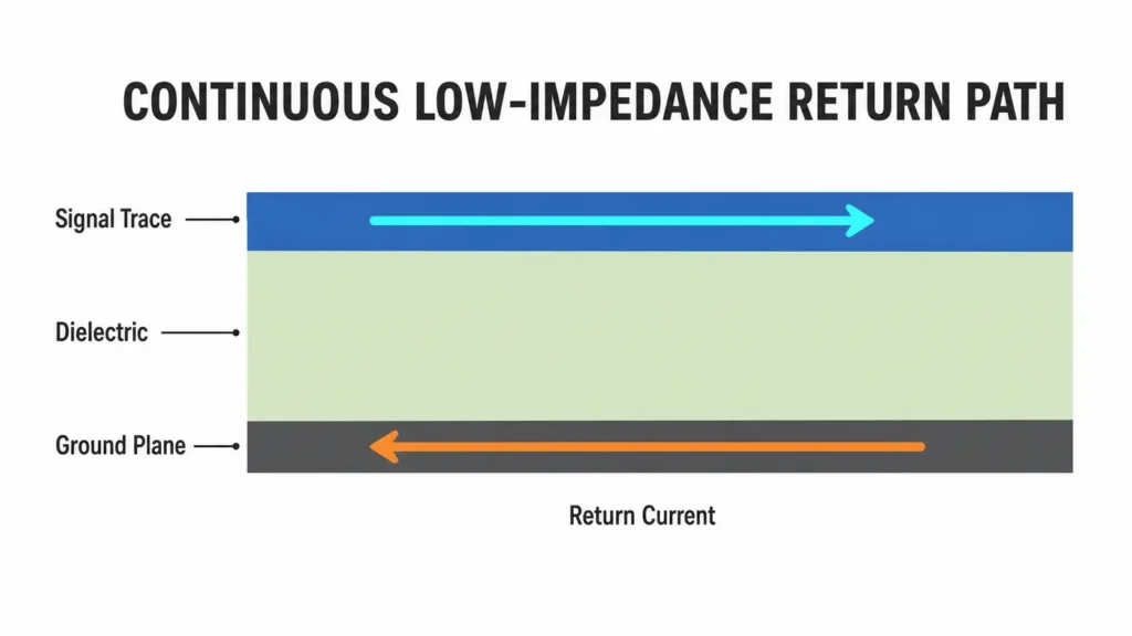
- Низкочастотные токи / токи постоянного тока: Постоянный ток следует по пути наименьшего сопротивления. На низких частотах ток распределяется по доступным медным проводникам в направлении источника.
- Высокочастотные токи: Переменный ток и быстрые цифровые переходные процессы следуют по пути наименьшей индуктивности (импеданса). Обратный ток протекает непосредственно под сигнальной дорожкой по смежному слою земли, образуя компактный контур, который минимизирует индуктивность контура и электромагнитное излучение.
- Ограничения по импедансу: Ток не следует строго по одной линии минимального сопротивления; он распределяется по всем доступным путям обратно пропорционально их импедансу ($Z = R + j\omega L$).
Почему GND важен?
Целостность сигнала, помехи и ЭМС
Слои земли и низкоимпедансные сети GND необходимы для поддержания целостности сигнала (SI) и электромагнитной совместимости (ЭМС).
- Дребезг земли: Когда несколько цифровых выходов переключаются одновременно ($di/dt$), скачки тока проходят через паразитную индуктивность ($L$) корпуса ИС и дорожек земли. Это генерирует кратковременный скачок напряжения на соединении с землей ($\Delta V = L \cdot \frac{di}{dt}$), известный как дребезг земли, который может вызвать ложное срабатывание логики.
- Перекрестные помехи: Без непрерывного слоя земли под высокоскоростными сигнальными линиями магнитные поля распространяются шире, наводя нежелательные помехи на соседние параллельные дорожки.
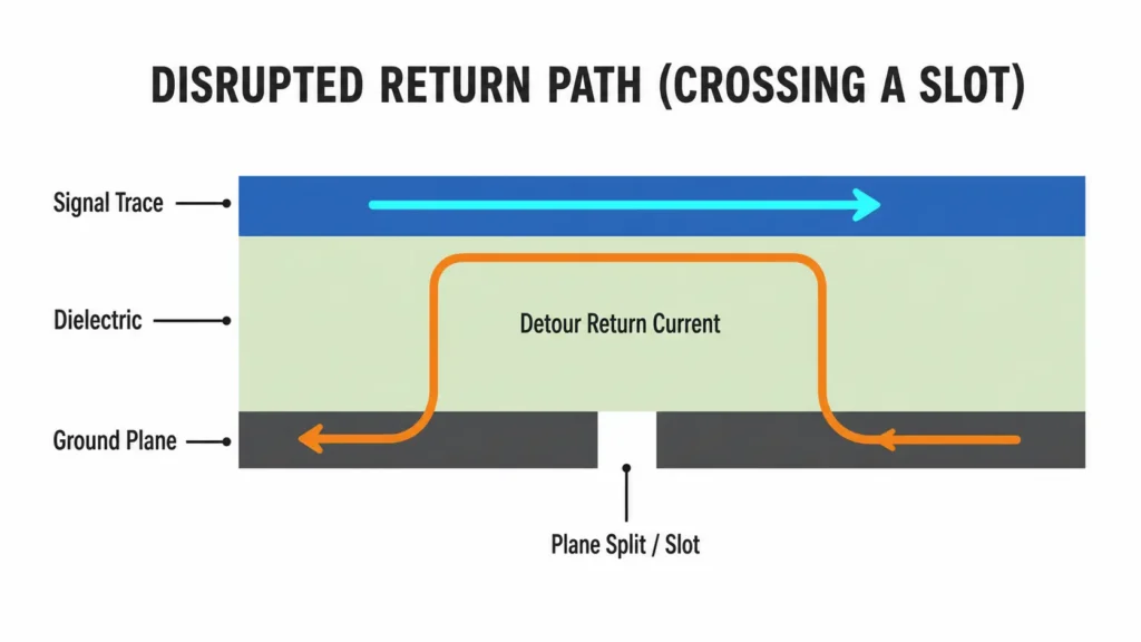
- Излучаемые помехи (ЭМИ): Нарушенные пути возврата тока увеличивают эффективную площадь контура высокочастотных сигналов. Непреднамеренные рамочные антенны излучают электромагнитную энергию, что приводит к несоответствию продукта нормативным требованиям ЭМС (таким как FCC или CE).
Роль надежности и безопасности
Критически важно различать узлы заземления, предназначенные для функциональной производительности, и те, что предназначены для безопасности человека:
- Функциональное заземление: Обеспечивает стабильность сигналов, чистоту внутренних шин питания и работу компонентов в пределах заданных допусков по напряжению.
- Защитное заземление (PE): Обеспечивает нахождение открытых токопроводящих поверхностей (например, металлического корпуса) под потенциалом земли. Если внутренний высоковольтный провод замыкает на корпус, защитное заземление безопасно отводит ток короткого замыкания непосредственно на землю, вызывая срабатывание автоматического выключателя или устройства защитного отключения (УЗО) до того, как оператор получит удар током.
Типы GND и когда их использовать
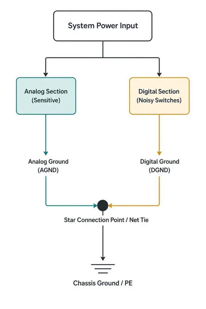
Заземление схемы/системы, сигнальное заземление и силовое заземление
- Системное заземление (System GND): Главный опорный узел 0 В для всей электронной сборки.
- Сигнальное заземление (SGND): Выделенные пути возврата, зарезервированные для слаботочных аналоговых или цифровых сигналов, для защиты их от высокочастотных помех переключения силовых цепей.
- Силовое заземление (PGND): Путь возврата для сильноточных нагрузок, включая импульсные стабилизаторы, драйверы двигателей, реле и силовые транзисторы. Высокие токи $di/dt$ в PGND генерируют скачки напряжения, которые должны быть изолированы от чувствительной логики.
AGND и DGND в смешанных платах
- Аналоговая земля (AGND): Зарезервирована для прецизионных аналоговых схем, таких как высокоразрядные АЦП, ЦАП, операционные усилители и источники опорного напряжения.
- Цифровая земля (DGND): Зарезервирована для высокоскоростной цифровой логики, микроконтроллеров, ПЛИС и интерфейсов памяти, которые загрязняют слои земли переходными помехами переключения.
Рекомендуемый подход к проектированию
Исторически разработчики часто прорезали физические щели в слоях земли печатных плат, чтобы разделить AGND и DGND. Однако современная практика проектирования высокоскоростных смешанных сигналов не рекомендует произвольное разделение слоев:
- Maintain a Solid Ground Plane: Use a single, continuous ground plane whenever possible.
- Implement Functional Component Placement: Group analog components together and digital components together in distinct physical regions of the PCB.
- Control Signal Routing: Ensure digital signals never cross into the analog region, and vice versa. This naturally isolates the return currents within their respective zones on the continuous ground plane without creating inductive ground slots.
- Targeted Net Ties: If an ADC datasheet specifically demands separate AGND and DGND planes, join them at a single physical point (using a Net Tie, 0 $\Omega$ resistor, or ferrite bead) directly underneath or adjacent to the IC.
Earth Ground, Chassis Ground, and Primary/Hot Ground
- Earth Ground (PE / EGND): Directly connected to physical soil via building earth rods. Used primarily for safety grounding and ESD dissipation.
- Chassis Ground: Connected to the structural metal frame or shell of an enclosure. Helps shield internal electronics from external radio frequency interference (RFI).
- Primary / Hot Ground: The zero reference point on the high-voltage AC side of an isolated power supply (e.g., after the mains bridge rectifier). WARNING: Hot ground is directly energized relative to Earth potential and presents a dangerous electric shock hazard.
| Ground Type | Schematic Symbol / Code | Primary Function | Main Noise / Hazard Risk | Best Practice Design Rule |
|---|---|---|---|---|
| System GND | Standard Signal Ground | General 0 V voltage reference | Common-impedance coupling | Keep traces low-impedance; use continuous ground planes |
| Signal GND (SGND) | Triangle / Wire Label | Low-current reference path | High-frequency signal distortion | Route adjacent to signal lines; isolate from heavy loads |
| Analog GND (AGND) | Clean Triangle / “AGND” | Reference for analog conversion | Digital switching noise | Spatial segregation; keep digital trace returns off AGND |
| Digital GND (DGND) | Earth-like or “DGND” | Return for logic switching | High $di/dt$ ground bounce | Decouple thoroughly at each IC pin; minimize trace loop areas |
| Power GND (PGND) | Heavy Fill Triangle | High-current power returns | Voltage drops and thermal dissipation | Use wide copper pours, heavy copper layers, and multiple vias |
| Protective Earth (PE) | Circle with 3 Horizontal Bars | Shock protection & fault clearing | High fault currents during insulation failure | Connect low-impedance to chassis; follow safety standards (UL/IEC) |
⚠️ SAFETY WARNING: High-Voltage Safety Boundary
Never bridge the Primary (Hot) Ground and Secondary (Cold) Ground of a mains-connected power supply using standard PCB traces or passive components that lack proper isolation ratings. Mains-connected primary circuits operate at lethal voltage levels. Measurements or modifications on the primary side must only be performed by qualified personnel using galvanic isolation transformers and specialized differential probes.
Is GND Positive or Negative?
GND is neither inherently positive nor inherently negative; it is simply the chosen zero-point (0 V) reference. The sign of any potential in a circuit depends entirely on its relationship to GND.
- Single-Supply Circuits (Standard Low-Voltage DC): In typical +5 V or +3.3 V digital systems, GND is connected to the negative terminal of the DC power supply or battery. Thus, the supply terminal is +5 V relative to GND.
- Dual-Supply Systems (Symmetric Rails): In precision audio amplification and operational amplifier circuits, power is supplied as +15 V, GND, and −15 V. Here, GND sits at the middle potential: the positive rail is +15 V above GND, while the negative rail is 15 V below GND.
- Positive-Ground Systems: Certain telecom networks and classic automotive systems use a positive-ground configuration (e.g., −48 V DC). In these designs, the positive power supply terminal is bonded to GND (0 V), making all functional operating rails negative with respect to ground.
How to Read GND Symbols on Schematics
Common Ground Symbols
Schematic diagrams use specialized ground symbols to distinguish between different electrical domains:
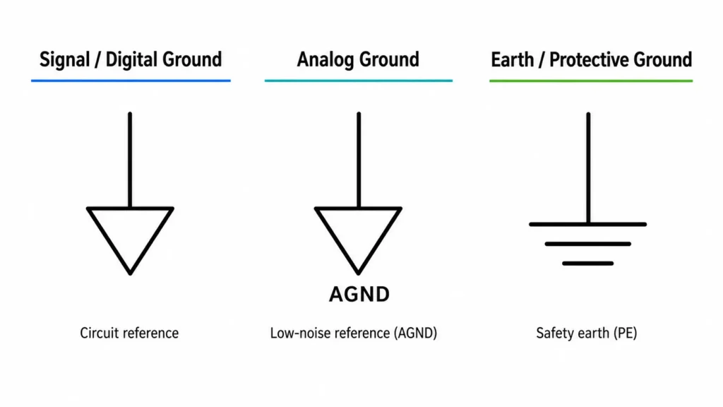
- Signal Ground / Earth Ground (Standard Triangle / Horizontal Bar): Standard 0 V reference for basic schematics.
- Earth Ground (3 Descending Bars in a Circle/Triangle): Represents a physical connection to Earth potential.
- Chassis Ground (Hatched Frame Symbol): Represents a connection to the equipment metal enclosure.
- Analog / Digital / Power Ground (Labeled Triangles): Differentiated by net names (
AGND,DGND,PGND) to indicate specific routing rules in PCB layout.
Read the Net Name Before Making a Connection
Schematic design software treats ground symbols as named global nets. If two ground symbols share the identical net name (e.g., GND), the CAD software will connect them together electrically.
- Distinct Net Names: Symbols named
AGNDиDGNDare treated as completely distinct nets by default. They will not be connected on the PCB unless explicitly joined using a Net Tie or zero-ohm resistor in the schematic. - Third-Party Modules: When interfacing with third-party microcontrollers or sensor breakout boards, always consult the official schematic. Do not assume all pins labeled “GND” share low-impedance internal connections on the module itself.
GND in PCB Design: A Practical Checklist
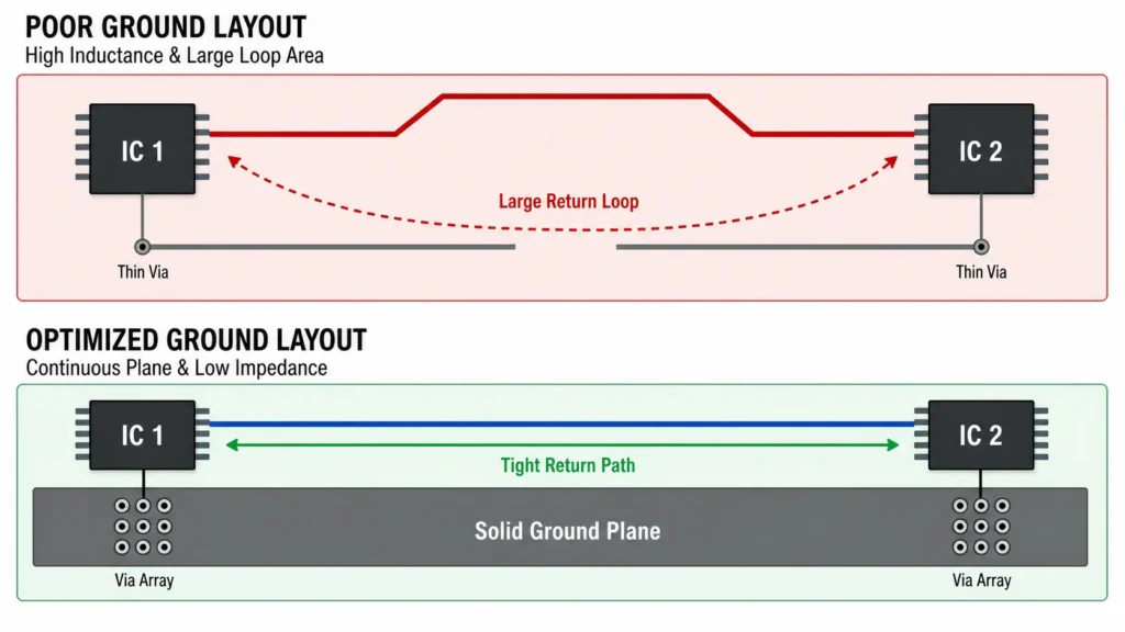
Keep Return Paths Continuous and Short
- Unbroken Reference Planes: Place high-speed traces on layers directly adjacent to an uninterrupted ground plane layer.
- Avoid Routing Across Slots: Never route a signal trace over a break, split, or slot in the adjacent ground plane. Crossing a slot forces the return current to take a long loop around the gap, creating high inductance, signal distortion, and excessive EMI.
- Minimize Return Loop Area: Keep high $di/dt$ loops (such as switching loops in DC-DC buck converters) as physically small as possible.
Place Decoupling Capacitors for the Loop
Decoupling capacitors serve as localized high-frequency energy reservoirs. To work effectively:
- Placement: Place decoupling capacitors as physically close as possible to the IC power (
VDD) and ground (GND) pins. - Low-Inductance Vias: Connect capacitor ground pads directly to the underlying ground plane using short, wide traces and dedicated vias placed close to the pads. Avoid long, thin traces that add unwanted parasitic inductance.
Manage Mixed-Signal and Power Returns Deliberately
- Functional Zoning: Group components logically into power, digital, and precision analog zones. Keep power switching return currents away from sensitive analog measurement paths.
- Thermal Relief Vias: Use stitched ground via arrays (via fencing) around high-frequency regions and under thermal pads of power ICs to conduct heat away to inner ground layers.
PCB GND Verification Checklist
[ ] 1. Continuous Ground Plane: Is at least one internal layer dedicated as an unbroken GND plane?
[ ] 2. Slot Crossing Check: Are high-speed traces routed strictly over solid copper without crossing split planes?
[ ] 3. Decoupling Loop Minimization: Are decoupling capacitors located immediately adjacent to IC power/ground pins?
[ ] 4. Switching Loop Area: Are high-power switching loops (e.g., DC-DC converters) laid out with minimal loop area?
[ ] 5. Ground Via Proximity: Do capacitor ground pads tie into the main plane with short, wide, low-inductance vias?
[ ] 6. Net Tie Inspection: Are distinct ground nets (e.g., AGND/DGND) tied deliberately at a controlled single point?
[ ] 7. Via Stitching: Are multiple ground vias placed around high-frequency areas and high-current return paths?
[ ] 8. Connectors and Shields: Are connector ground pins and chassis shield pads properly tied to chassis/PE ground?
Common GND Problems and How to Troubleshoot Them
Symptoms and Likely Causes
| Symptom | Probable Cause | Corrective Action |
|---|---|---|
| 50 Hz / 60 Hz Hum in Audio | Ground Loop (multiple ground paths forming a loop that picks up line magnetic fields) | Break the ground loop using balanced audio connections, ground-lift switches, or isolation transformers. |
| ADC Readings Jitter / Unstable Data | Common Impedance Coupling (digital switching noise sharing ground paths with analog inputs) | Segregate analog and digital floor placement; ensure digital switching currents do not flow across the analog ground plane. |
| System Resets During Switching | Ground Bounce ($di/dt$ noise creating transient logic-level shifts) | Add local high-frequency decoupling capacitors; minimize ground connection inductance; use a solid ground plane. |
| High EMI / Fails EMC Testing | Disrupted Return Paths (traces crossing split planes or long return loops) | Eliminate plane splits under high-speed traces; add stitching capacitors or vias across necessary boundaries. |
| Enclosure Shocks Operator | Missing or Compromised Protective Earth Connection | Immediately disconnect power; inspect safety ground continuity from metal chassis to wall plug PE pin. |
Safe Low-Voltage Troubleshooting Workflow
- Power-Off Continuity Inspection: Disconnect power entirely. Set a Digital Multimeter (DMM) to resistance/continuity mode. Check resistance between sub-system ground points. High resistance indicates poor connections, cold solder joints, or missing ground vias.
- DC Offset Check: Apply power to the low-voltage circuit. Measure DC voltage between different ground locations (e.g., between sensor ground and MCU ground). Ideally, the DC potential difference should be near 0.00 V. Any measurable offset indicates high ground resistance carrying current.
- Oscilloscope Ground Lead Caution: Standard benchtop oscilloscope probe ground clips are internally connected directly to Earth Ground through the scope’s power cord. NEVER connect a standard oscilloscope probe ground clip to an unisolated, floating, or hot ground point; doing so will cause a short circuit, destroy equipment, or trip main breakers. Use differential probes for floating measurements.
FAQs About GND
What does GND stand for in electronics?
GND stands for Землю. In electrical engineering, it represents the zero-volt (0 V) baseline reference potential used for measuring system voltages and completing current return paths.
Is GND the same as negative?
Not necessarily. While GND is tied to the negative terminal of a battery in common single-supply DC circuits, GND is simply an arbitrary reference point. In dual-supply systems (+15 V / 0 V / −15 V) or positive-ground systems (−48 V), GND is separate from the negative power terminal.
Is GND the same as earth or ground wire?
No. Circuit GND refers to the local reference plane of an electronic device, which can float independently (e.g., in an airplane or phone). Earth ground (PE) specifically refers to a physical connection to the earth’s surface for safety fault protection.
Does GND always carry current?
Yes. Electrical current must travel in a closed loop back to its power source. Circuit GND serves as the primary return path for operational current. Protective Earth (PE) ground, however, should carry no current during normal operation, conducting only during electrical fault conditions.
What is the difference between GND and neutral?
In AC utility wiring, the Neutral wire is a current-carrying conductor that completes the circuit back to the electrical panel, bonded to Earth at the service entrance. GND (Protective Earth) is a safety conductor that normally carries no current and serves to clear fault currents safely.
Why do AGND and DGND have different names?
They are named separately to force schematic design software to treat them as distinct nets. This prevents designers from mixing noisy digital switching currents with sensitive analog measurement return paths on the PCB layout.
Can two devices work without a shared GND?
Only if they use galvanically isolated interfaces (such as optocouplers, transformers, or wireless links). Direct multi-wire data communication (like UART or SPI) requires a shared ground reference to interpret signal voltages accurately.
What happens if GND is disconnected?
Disconnecting GND breaks the electrical return path, halting circuit operation. In ungrounded systems, floating voltages can rise unpredictably to supply potentials, potentially damaging sensitive electronics or creating electric shock hazards.
What does GND mean on a power supply or connector?
On a DC power supply or connector terminal, GND indicates the 0 V reference terminal for power delivery and signal outputs. On an AC supply, it often denotes the chassis/Earth safety ground connection.
How do I test a GND connection safely?
For unpowered low-voltage circuits, measure continuity using a DMM set to ohms. For live mains equipment, safety ground testing must be performed using dedicated earth-loop impedance testers by qualified personnel.
Основные выводы
- GND is a Relative Reference: GND is defined as the 0 V reference point for a circuit, but it is not inherently at absolute Earth potential, nor is it strictly identical to a negative power terminal.
- Current Returns to the Source: Functional GND networks carry operational return currents. High-frequency return currents automatically follow the path of minimum inductance directly beneath signal traces.
- Prioritize Ground Integrity in PCB Design: Use continuous ground planes, place decoupling capacitors close to IC power pins, avoid routing traces across split planes, and segregate analog and digital layouts systematically.
To deepen your understanding of PCB layout and circuit safety, explore related design guides on PCB Ground Planes, EMI/EMC Mitigation Strategies, Decoupling Capacitor Selection, и Multimeter Safety Category Ratings.
