Controlled impedance is the practice of designing and manufacturing PCB traces so their characteristic impedance meets a specified target and tolerance. The result depends on the conductor geometry, dielectric construction, and reference planes. A complete requirement also states how the manufacturer will verify the finished structure.
A note that says only “50 ohms” leaves important decisions open. Which nets and layers does it cover? Is the target single-ended or differential? May the fabricator change trace width? What constitutes a passing measurement?
Those decisions connect the circuit design to the production order. Agree them before releasing the board.
Key Takeaways
- Evaluate signal edge time and propagation delay; clock frequency alone does not determine the need for impedance control.
- Specify the impedance mode, net class, signal layer, reference planes, target, and tolerance together.
- Confirm finished trace geometry against the actual material construction and production stackup.
- Agree the coupon, TDR method, measurement window, sampling, and acceptance rule before fabrication.
- A passing coupon supports process verification. It does not certify every routed net or complete channel.
When does a PCB trace need impedance control?
Use PCB impedance control when the interface requires it or when transmission-line effects matter to the signal. Start with the device’s layout guidance and electrical requirements, then compare route flight time with the fastest relevant rise or fall time.
Compare edge time with propagation delay
A clock’s repetition rate and its edge time describe different things. Two drivers running at the same clock frequency can have very different rise times. Tektronix’s Probe Card Tutorial distinguishes repetition frequency from the bandwidth needed to preserve pulse shape. Faster edges require attention to higher-frequency content.
For an illustrative calculation, assume a propagation velocity of 150 mm/ns:
One-way delay = route length ÷ velocity = 30 mm ÷ 150 mm/ns = 0.2 ns.
That delay is a much larger fraction of a 0.5 ns edge than of a 5 ns edge. The assumed velocity is an example input, not a universal FR-4 property. Use the actual stackup’s delay when assessing the design. There is no single clock-frequency cutoff that covers every board.
Follow interface and device requirements
Record the required impedance, tolerance, routing topology, and termination scheme for each interface. Check the specific device and interface revision. Avoid carrying a target from one generation or topology into another without checking it.
Also examine layer changes, reference-plane gaps, connectors, and vias. Controlling a long uniform trace does not remove discontinuities elsewhere in the signal path.
Single-ended impedance, differential impedance and matching
Specify the impedance mode before specifying the number. A 50-ohm single-ended line and a 100-ohm differential pair describe different electrical structures, even when their numerical relationship looks convenient.
| Requirement | What it describes | What to specify |
|---|---|---|
| Single-ended impedance | One signal conductor relative to its reference structure | Signal layer, reference plane, trace geometry, target and tolerance |
| Differential impedance | A pair driven with equal and opposite signals | Both traces, edge-to-edge pair gap, reference structure, target and tolerance |
| Impedance matching | The relationship between source, interconnect and load | Driver behavior, line impedance, load and termination strategy |
Coupling changes the differential result
Differential impedance is not automatically twice the single-ended impedance of an isolated trace. The pair’s fields interact, and spacing affects the result. A solver may report odd-mode impedance for opposite-polarity excitation or even-mode impedance for same-polarity excitation. Check which quantity it reports before transferring a number to the fabrication drawing.
A compliant trace can still reflect a signal
Impedance control establishes the manufactured line’s properties. Matching addresses the system around that line. A trace can meet its fabrication target while an unsuitable termination or connector still produces reflections.
Texas Instruments’ PCB trace impedance matching lesson explains how geometry determines trace impedance and how driver-to-trace matching affects rise time, overshoot, and ringing. Choose termination from the actual driver, load, and topology rather than adding a resistor simply because a trace has a named impedance.
How stackup and trace geometry set characteristic impedance
Trace width has meaning only within a defined cross-section. The same width can produce different impedance on two stackups because the field geometry and dielectric properties differ. Analog Devices’ Design Reliable Digital Interfaces for Successive-Approximation ADCs identifies the transmission-line model, dielectric properties, conductor dimensions, and spacing as impedance-calculation inputs.
Microstrip and stripline reference structures
Microstrip runs on an outer layer above a reference plane. Its fields extend through the substrate and surrounding material, including any solder mask. Stripline runs inside the board between reference planes, with fields contained within the dielectric structure.
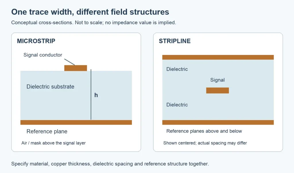
A continuous reference plane provides the intended return-path structure. A split or missing reference beneath the route changes that structure. Where a signal changes layers, its return path also needs attention; a uniform cross-section calculation does not model the entire transition.
Material properties, finished copper and mask
Use the laminate construction and dielectric properties appropriate to the analysis frequency. Dk is the material’s relative permittivity, often called its dielectric constant. “FR-4” identifies a material family, not one fixed Dk. The PCB material properties and selection guide explains why construction and operating requirements matter.
Sierra Circuits’ Why Controlled Impedance Really Matters explains the effects of width, dielectric spacing, and Dk. For a defined geometry, with other inputs fixed:
| Change | General effect | Qualification |
|---|---|---|
| Increase trace width | Lowers characteristic impedance | Model the finished etched cross-section |
| Increase trace-to-reference distance | Raises impedance | Keep the other reference relationships consistent |
| Increase dielectric constant | Lowers impedance | Use suitable material/construction data |
| Reduce pair spacing | Generally lowers differential impedance | Coupling depends on the full geometry |
| Change copper thickness or mask | Changes impedance | Include the actual finished structure in the model |
Specify dielectric spacing to the reference plane, not just total board thickness. For outer conductors, distinguish starting foil from finished plated copper. Etching can also leave a trapezoidal conductor rather than the rectangular shape used in a simple calculation.
What an impedance calculator can estimate
Use the PCB impedance calculator for initial sizing and sensitivity checks. Record its geometry and assumptions. An empirical estimate does not replace fabrication review of the production construction.
Ask the manufacturer to confirm available materials, pressed dielectric thicknesses, finished copper, and achievable geometry. The FR-4 PCB manufacturing page describes controlled-impedance support subject to engineering review. Establish that construction before routing dense areas around a trace width that may need to change.
Write a controlled impedance fabrication specification
A usable specification connects electrical requirements to identifiable nets and physical structures. Put those requirements in a controlled drawing or table and keep its revision aligned with the fabrication data.
Fill in the impedance table
The following hypothetical handoff example illustrates the record format. Its dimensions are invented example entries, not solved geometries: they do not demonstrate that the stated targets will be met. Both rows remain on engineering hold until a fabricator supplies a verified construction and the design owner approves it.
| Field | Example A | Example B |
|---|---|---|
| Net class | CTRL_SE | DATA_DIFF |
| Signal layer | L1 | L1 |
| Reference plane | Continuous L2 ground | Continuous L2 ground |
| Mode and target | Single-ended, 50 Ω | Differential, 100 Ω |
| Contract tolerance | ±10%, illustrative | ±10%, illustrative |
| CAD trace width | 0.150 mm | 0.150 mm per trace |
| Proposed finished width | 0.160 mm, unverified | 0.160 mm per trace, unverified |
| Pair edge-to-edge gap | Not applicable | 0.150 mm, unverified |
| Construction record | STACK-A, revision A; proposal required | STACK-A, revision A; proposal required |
| Adjustment permission | None before written approval | None before written approval |
| Verification request | Representative single-ended coupon and report | Representative differential coupon and report |
| Release status | HOLD | HOLD |
Download the blank impedance handoff template and the illustrative filled example to adapt the records to your project.
The construction record should identify laminate/prepreg, relevant Dk and its basis, dielectric distances, finished copper thickness, and mask assumptions. Record the finished width proposed by the fabricator separately from the CAD artwork width. Include trace identifiers when a net uses several geometries or layers.
Pair gap means the edge-to-edge space between the two conductors. Clearance from that pair to unrelated copper is a separate routing constraint.
Agree which changes require approval
A manufacturer may propose width, gap, or dielectric changes to meet the target. Decide what is allowed before production. A width change can affect pad entries and routing clearances; a gap change can affect coupling and the available corridor.
Use a fabrication note such as:
Apply impedance requirements only to the listed net classes and layer/reference combinations. Submit the proposed production stackup, finished geometry, and verification plan for written approval before fabrication. Changes to material, dielectric spacing, copper, reference structure, width, or pair gap require approval unless an explicit permitted range is recorded.
This is a starting instruction, not a substitute for the project’s manufacturing agreement. Check that the approved values reach the production data and coupon definition. The PCB fabrication submission requirements identify the Gerber, drilling, stackup, and drawing information needed for review.
Verify impedance with coupons and TDR testing
Time-domain reflectometry, or TDR, uses reflections from an electrical step to assess impedance along a structure. Define the test method and decision rule alongside the target; “100 ohms ±10%” does not describe the whole test.
What an impedance test coupon demonstrates
A coupon is a dedicated test structure associated with the production panel. Its value comes from representing the relevant layer, conductor geometry, dielectric construction, and reference structure.
Polar Instruments’ guidance on test coupons and built-in test traces explains why actual-board measurements can be complicated by vias, branches, plane gaps, and probe access. It also emphasizes the need for representative coupon structures.
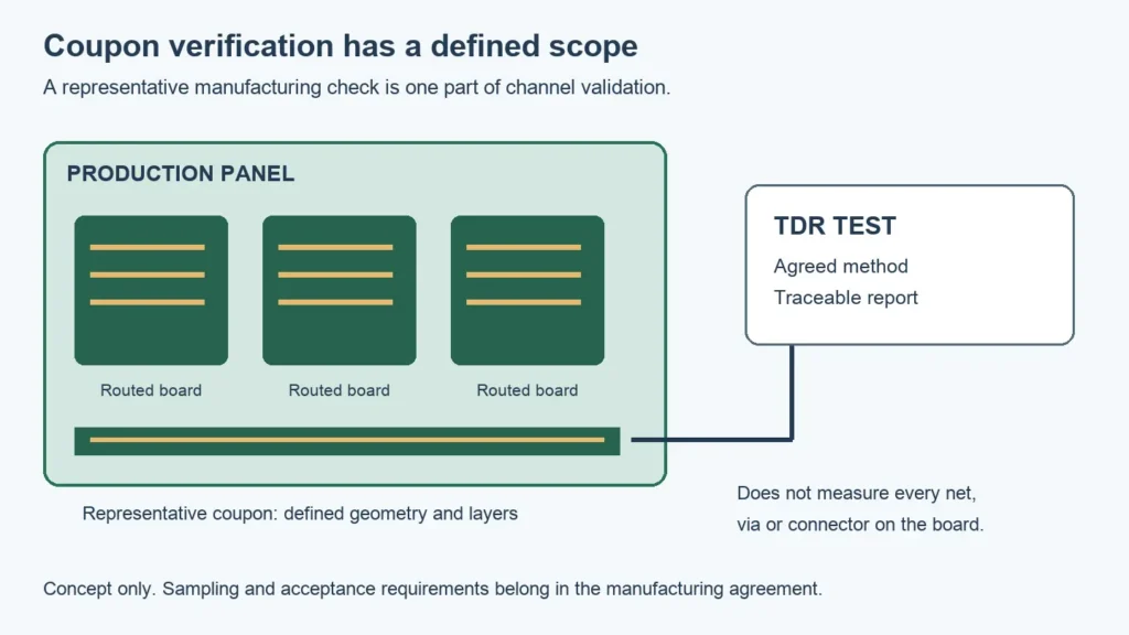
A coupon result therefore supports a defined manufacturing check. It is not a direct measurement of every net on every board. A passing coupon cannot establish that a discontinuity in a connector or layer transition is acceptable.
Define the measurement and acceptance rule
Agree these details before ordering:
- Coupon identifiers, representative layers, geometries, and panel/lot traceability.
- Calibration, probe/fixture arrangement, and differential setup where applicable.
- Delivered test edge, usable measurement window, and treatment of launch/end effects.
- Reported statistic, acceptance limits, and treatment of measurement uncertainty.
- Sampling plan, report contents, and disposition of failed or ambiguous results.
Tektronix’s TDR Test explains how measurement bandwidth and interconnects affect the delivered rise time, and how multiple reflections can distort apparent impedance in complex structures. A faster instrument setting alone does not establish the resolution at the coupon.
Worked example: a 100-ohm differential requirement
Assume the customer and fabricator agree on 100 Ω differential with ±10% tolerance. The numerical limits are:
Lower limit = 100 × 0.90 = 90 Ω. Upper limit = 100 × 1.10 = 110 Ω.
For this arithmetic example, assume an approved measurement window and a reported value assessed directly against inclusive limits, with no guard band. This is an illustrative decision rule, not a recommended universal uncertainty policy.
| Illustrative reported value | Decision under that rule | Next action |
|---|---|---|
| 103 Ω | Passes the numerical criterion | Retain the traceable result with the agreed inspection records |
| 112 Ω | Fails the numerical criterion | Hold acceptance and investigate under the agreed disposition process |
These are synthetic values, not production results. Use the customer’s tolerance and agreed measurement procedure on a real order. If uncertainty requires guard bands or an indeterminate category, apply that policy instead of this simplified rule. Do not accept or reject a coupon from an arbitrary point near a probe launch.
Common reasons a calculated design misses its target
When a model and measurement disagree, compare their inputs and structures before changing the artwork. A nominal calculation, an approved production model, and a measured coupon may describe different cross-sections.
| Potential cause | What to check | Prevention |
|---|---|---|
| Generic material data | Dk, frequency basis and laminate construction | Agree the material record used for the model |
| Wrong copper assumption | Starting foil versus finished copper and etch shape | Model the production conductor |
| Changed dielectric spacing | Pressed thickness and reference-plane assignment | Review the final stackup revision |
| Wrong geometry model | Outer/inner layer, symmetry, mask and pair arrangement | Match the model to the actual cross-section |
| Pair gap changed | Finished edge-to-edge spacing and routing exceptions | Control both width and gap in the release |
| Unapproved substitution | Material and process changes | Require documented approval |
| Misleading test region | Launch artifacts, end reflections or setup error | Use the agreed method and valid window |
Keep process verification separate from channel troubleshooting. If coupons pass but the link fails, inspect actual routing, return paths, transitions, termination, and connector behavior. Changing all trace widths can obscure the original problem and create new mismatches.
Controlled impedance FAQ
Is controlled impedance the same as controlled dielectric?
No. Controlled dielectric specifies aspects of the dielectric construction or spacing. Controlled impedance specifies an electrical target for a defined conductor/reference structure. Dielectric control helps make impedance predictable, but width, copper, material properties, mask, and pair coupling also matter. State which result the supplier must deliver and verify.
Does a continuity test verify impedance?
No. An open/short or continuity test checks connectivity. It does not establish the trace’s transmission-line impedance. A conductor can connect the correct pads and still miss its impedance target. Specify the required impedance test separately from the board’s electrical connectivity inspection.
Is ±10% always the required tolerance?
No. Tolerance comes from the applicable design requirements and manufacturing agreement. The ±10% values here illustrate specification and acceptance arithmetic. They are not a universal standard or a guaranteed supplier capability. Confirm whether the requested tolerance is achievable for the selected construction and verification method.
Does a passing coupon prove every routed net passes?
No. It supports the sampled structure under the agreed test and sampling plan. It does not measure every net or validate every discontinuity. Maintain coupon-to-panel traceability, then assess the actual channel against its separate signal-integrity and interface requirements.
What should I send for a manufacturing review?
Send fabrication and drill data, net classes, layer/reference assignments, target/mode/tolerance, proposed stackup, and drawing revision. Include test, sampling, report, and change-approval requirements. Resolve differences between CAD geometry and proposed finished geometry before production release.
For a project review, submit your stackup and impedance requirements, including the verification plan you need the manufacturer to confirm.