A multilayer PCB contains three or more conductive copper layers separated by insulating dielectric and bonded into one board. The count refers to copper layers, not prepreg, core sheets or solder mask. It does not, by itself, tell you whether the board is rigid or flexible, how thick it is or how well it will perform.
Choosing a construction means comparing the signals, their return paths, routing space and fabrication constraints. The fictional measurement board below carries the same requirements through two-, four- and six-layer options so the outstanding decisions are visible. For the mechanical and material choices behind a rigid board, see the rigid PCB construction guide.
Key Takeaways
- Layer count, mechanical construction and finished thickness are separate specifications.
- A two-layer board can be viable when the design meets its requirements; four and six layers offer other ways to assign copper and routing.
- Check return paths, reference-plane continuity and layer transitions against the actual geometry and power distribution network.
- Cost depends on the complete build. Additional copper layers do not automatically require another lamination cycle.
- The example is fictional; all candidates and the required human engineering review remain pending.
What Is a Multilayer PCB?
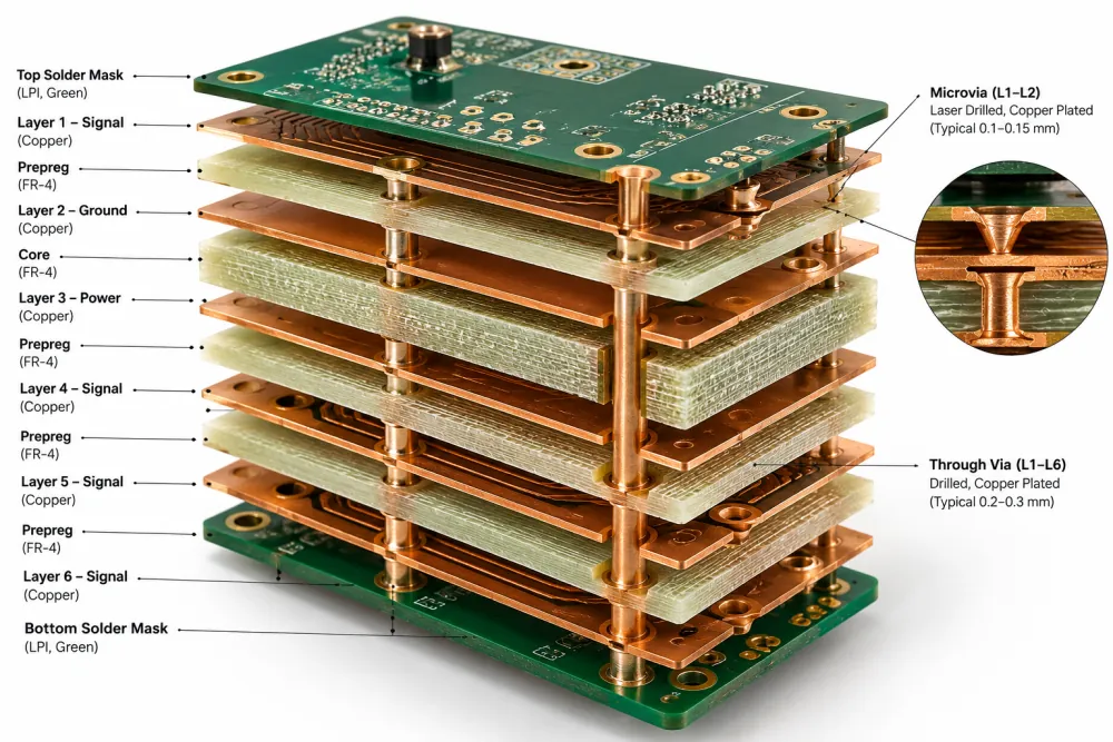
A single-sided PCB has one copper layer; a double-sided PCB has two. A multilayer circuit board has three or more copper layers. Even counts are common, but odd counts are possible. The layers may carry signals, power or ground, depending on the design.
Layer count describes electrical construction, while rigid, flex and rigid-flex describe mechanical construction. A multilayer board can use any of those mechanical forms. Its finished thickness depends on the actual copper and dielectric construction, so a layer count alone does not specify it.
The flex PCB construction guide covers flexible materials and mechanical design.
2-Layer vs 4-Layer vs 6-Layer PCB: What Changes?
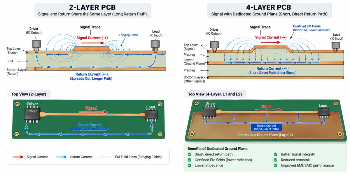
The examples below compare possible layer assignments, not standard recipes. A reference plane is a copper region that provides a path for signal return current; its usefulness depends on the geometry and continuity of that region. On a small screen, scroll the table sideways to see all columns.
Layer-count comparison
| Candidate | Example copper roles | Routing and reference considerations | Fabrication consideration | When to evaluate |
|---|---|---|---|---|
| 2 layers | Signal and ground copper on both sides as needed | Routing can interrupt available ground copper. Check each critical return path. | No internal copper layers; actual complexity still depends on the features and tolerances. | When placement, routing and electrical requirements may fit on two sides. |
| 4 layers | Signal / ground / power / signal | Two outer signal layers, with inner copper available for references and power. Check the power-plane reference and transitions. | Inner layers need alignment; material and thickness choices remain open. | When internal ground and power regions merit comparison with a two-layer layout. |
| 6 layers | Signal / ground / signal / power / ground / signal | An additional proposed signal layer creates routing choices. Its return can involve both adjacent planes. | More internal copper requires a suitable construction and alignment plan. | When routing or reference needs suggest evaluating another signal layer. |
More layers do not guarantee lower emissions, controlled impedance or a smaller board. A two-layer design can work if its actual routing, electrical behavior and other requirements are acceptable. All three candidates need layout and fabrication review.
How a Multilayer Circuit Board Is Built
A multilayer board combines patterned copper with insulating materials, then uses plated connections where the design calls for layers to connect.
Copper, core and prepreg
Copper forms traces, pads and planes. A core is a cured laminate, often supplied with copper on its faces. Prepreg is reinforcement impregnated with partially cured resin; it bonds layers during lamination. The number and arrangement of cores, prepregs and copper foils depend on the selected construction. A stackup drawing records their order and the specifications needed to build the board.
How vias connect selected layers
A plated through-hole spans the board. A blind via connects an outer layer to an internal layer, while a buried via connects internal layers without reaching either surface. Siemens’ 2025 explanation of blind and buried vias describes these structures and the manufacturing tradeoffs they can introduce.
A plated barrel passing through an internal layer does not automatically connect to its copper. Pads and clearances determine which layers it joins. Choose via spans with the fabricator’s process and design rules in mind; the PCB via guide covers the options, and the HDI PCB guide addresses buildup and microvia structures.
Reading a 4-Layer PCB Stackup and a 6-Layer Stackup
Read a stackup from one board surface to the other, assigning a purpose to every copper layer. These two examples show proposed roles, not finished fabrication stackups. Plane shapes, dielectric geometry and connections still need design work.
Four-layer PCB stackup
One candidate is L1 signal / L2 ground / L3 power / L4 signal. Where L2 ground is continuous and the geometry supports it, it can provide a nearby reference for L1 signals. L4 signals lie next to L3 power; their return paths depend on the power copper’s continuity, geometry and power distribution network. Altera’s power and ground layer guidance describes using either power or ground as a reference and explains why discontinuities in power copper need attention.
A signal changing layers may also change references. Evaluate how its return current transfers between the relevant reference regions, including the power network and the placement and impedance of decoupling. Eric Bogatin’s discussion of reference-plane transitions explains why the plane connection and capacitor impedance matter. A capacitor’s presence alone does not prove that the transition is acceptable. Power-plane gaps or islands also need attention.
Analog Devices’ 2022 mixed-signal layout guidance discusses a four-layer example and return-path considerations for high-performance data acquisition. It is useful context, not a universal minimum layer count.
Six-layer PCB stackup
Another candidate is L1 signal / L2 ground / L3 signal / L4 power / L5 ground / L6 signal. L1 and L6 are adjacent to ground layers, which can serve as references where the actual copper and geometry support them. L3 is bounded by L2 ground and L4 power: its fields and return currents can involve both planes, depending on their geometry and the power distribution network.
Review the paths for each signal and each transition, rather than assuming layer labels establish continuity. Ask the fabricator about stackup symmetry and copper distribution as mechanical and manufacturing checks; symmetry alone does not guarantee flatness. If impedance control is required, the controlled impedance PCB guide covers specifications and verification.
Worked Example: Choosing Layers for a Compact Measurement Board
This teaching example compares the same fictional requirements across all three candidates. No customer board, measured result or completed design review is implied.
State the requirements and assumptions
Suppose a rigid mixed-signal board must fit a 55 × 40 mm outline, sample a 0–2 V sensor signal up to 100 Hz with a 16-bit analog-to-digital converter, and communicate over a serial peripheral interface (SPI) link with a 1 MHz clock. For this exercise, allocate the board at most 1 mV root-mean-square (RMS) noise referred to the converter input within a nominal 0–100 Hz measurement band. Assume the sensor connector and converter can be placed on the same side, with the SPI connector toward the opposite board edge. The provisional finished thickness is 1.6 mm, subject to enclosure and connector fit. These values are invented design targets, not measurements or requirements for a particular product.
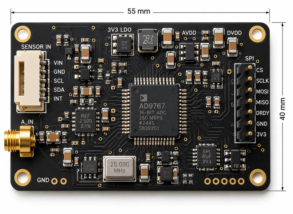
If the converter’s full-scale range is 2 V, one ideal 16-bit code step is approximately 2 V / 65,536, or 30.5 microvolts at the converter input. In that case, the allocated 1 mV RMS, referred to the same input, is approximately 33 code steps RMS. A code step is a voltage interval, while RMS noise describes noise magnitude over the stated band. The noise allocation must be judged against the actual measurement resolution and accuracy needs; this comparison alone does not establish effective resolution or a measurement result. The sensor’s 0–2 V signal range does not by itself establish the converter’s full-scale range.
Actual component selection, sensor impedance, supply noise, edge rise and fall times, component locations, signal routes and lengths, plane shapes, routing density, temperature, available fabrication stackups, connector tolerances and test requirements are unknown. Specify the measurement setup, bandwidth and operating conditions before testing the noise target. Converter resolution alone does not establish measurement accuracy, and the SPI clock rate alone does not establish the edge speed or whether impedance control is needed.
Compare the candidates
Each row applies the same outline, sensor signal, noise target, interface and provisional thickness above. Copper roles and return paths are proposals to investigate, not claims that the board will route or pass a test. On a small screen, scroll the table sideways to see all columns.
Worked example comparison
| Candidate and proposed copper roles | Possible return path | Routing and open checks | Possible manufacturing tradeoff | Approval |
|---|---|---|---|---|
| 2 layers: L1 signals and ground fill; L2 ground where possible, with signals as needed | Return paths depend on the complete circuit and frequency-dependent impedances; traces and holes can interrupt ground copper[cite: 2]. | Test whether sensor and SPI routes fit while preserving a suitable ground path; define and verify the 1 mV RMS noise target[cite: 2]. | No inner copper; fine features or tight tolerances may still affect the build and quote[cite: 2]. | Pending[cite: 2] |
| 4 layers: L1 signal / L2 ground / L3 power / L4 signal | L1 may reference L2. L4 may reference L3; transitions need a suitable path through the power distribution network[cite: 2]. | Check whether sensor routing can use L1 over continuous L2, whether SPI fits and whether noise, L4 returns and thickness meet requirements[cite: 2]. | Inner-layer registration and a construction meeting the 1.6 mm target need review[cite: 2]. | Pending[cite: 2] |
| 6 layers: L1 signal / L2 ground / L3 signal / L4 power / L5 ground / L6 signal | L1 and L6 are next to ground; L3 lies between ground and power and its return can involve both[cite: 2]. | Check whether SPI or other routes need the extra layer, then assess L3, transitions, thickness and the same noise target[cite: 2]. | More internal copper and alignment requirements may affect construction and cost; confirm the available process[cite: 2]. | Pending[cite: 2] |
Carry the four-layer candidate forward provisionally because the sensor and converter could be placed on L1 over an L2 ground region, while other routes use the remaining space. The separate power layer is another feature to evaluate. This is a layout hypothesis, not evidence that the noise target or any other requirement passes. Two layers remain viable if a real layout meets the same electrical and mechanical requirements. Review six layers if routing or reference needs justify another signal layer and a suitable construction is available.
Record the review decision
Use a short decision record to keep assumptions from becoming an accidental approval:
- Requirement: The fictional outline, sensor signal, noise objective, converter, SPI clock and provisional thickness above apply to every candidate. Other performance limits and a test method remain to be defined.
- Candidate and rationale: Four layers are provisionally carried forward for evaluation of ground, power and routing. Two and six layers remain alternatives.
- Status and reviewer roles: Design review and approval are pending for all three candidates. Intended review roles include the board designer, electrical or signal-integrity reviewer, mechanical engineer and fabricator; no reviewer has been appointed in this example.
- Missing verification: Obtain device requirements and edge times, a real placement and routed geometry, return-path and power-network analysis, an available stackup, thickness and connector tolerances, and agreed tests. Revise a candidate if its routing interrupts a needed return path or fails a requirement.
- Noise-test plan: Before comparing candidates, agree the sensor input condition or representative source impedance, operating conditions, sampling and filtering. Define the practical lower frequency limit or observation time, treatment of slow drift, and effective measurement bandwidth consistent with the nominal band. Specify which noise sources are included in the board allocation, including how sensor and test-equipment noise will be handled. Define how to calculate RMS noise referred to the converter input over that band. Against the example’s allocated limit, a result at or below 1 mV RMS is a pass for that noise criterion only; no result exists yet.
- Approval condition: Responsible engineers must check the chosen design against actual requirements, and the intended fabricator must confirm the proposed construction before the design can be released.
A qualified human engineer must separately review this educational example, its layer roles and the diagrams before publication. That review is pending and would not approve a board for manufacture.
Multilayer PCB Manufacturing: From Inner Layers to Test
A conventional rigid multilayer fabrication sequence forms the internal circuits, bonds the stack and then creates the outer circuits and connections. The order and inspection points vary with the design and supplier. Flex and rigid-flex constructions can use flexible bondply and coverlay, with a process specific to their materials and design.
- Prepare inner layers. Image and etch the required inner copper patterns, then inspect them before they become enclosed.
- Align and laminate. Arrange cores, prepreg and outer copper, register the layers, and bond the stack under heat and pressure.
- Drill and metallize. Make the specified holes and plate the applicable barrels to provide designed connections.
- Form the outer circuits. Image, plate and etch the outer copper as required by the process, then apply solder mask and the specified surface finish.
- Profile, inspect and test. Form the board outline and perform the inspections and electrical tests agreed for the order.
Eurocircuits’ registration guidance explains why the alignment of layers and drilled features matters. Its production inspection sequence illustrates checkpoints in one manufacturer’s process; it does not establish another supplier’s tolerances or test scope.
Some blind or buried structures need staged processing and sequential lamination. Several copper layers can also be combined in one lamination cycle, so adding layers does not invariably add another cycle. An agreed open/short test checks connectivity and isolation within its scope; it does not establish complete signal integrity, thermal performance or product qualification. Assembly adds components and is a separate scope; the industrial PCB production guide describes that wider workflow.
Multilayer PCB Design Checks Before Release
Review the actual layout and proposed stackup together before releasing fabrication files:
- References and transitions: Examine copper continuity near critical signals, gaps, layer changes and the relevant power-network paths. Analyze crossings of plane splits in the actual geometry.
- Materials and geometry: Confirm laminate, dielectric spacing, copper requirements and finished thickness with the fabricator. If controlled impedance is required, specify the nets, targets and tolerances and agree how to verify them.
- Copper and registration: Review layer symmetry, copper distribution, pads, clearances and alignment tolerances for the proposed process.
- Vias and holes: Check hole types, sizes, spans and intended connections against the stackup and supplier’s rules.
- Mechanical fit: Check the outline, thickness tolerance, mounting and connectors against the enclosure and assembly requirements.
- Acceptance: Agree inspection and electrical-test scope, plus any thermal, environmental or functional checks needed for the product.
A completed checklist should point to actual layout and supplier evidence, not just layer names. Record unresolved items and their owners before release.
What Drives Multilayer PCB Cost?
Multilayer PCB cost depends on the complete construction and order, rather than copper-layer count alone.
Cost factors
| Factor | Possible consequence to discuss in a quote |
|---|---|
| Layer count and board area | Additional inner layers can require more material, imaging and inspection. Larger boards can reduce the number that fit on a fabrication panel. |
| Laminate and thickness | A specialized laminate or tight finished-thickness tolerance may narrow material and stackup choices, affecting material or processing cost. |
| Via type and span | Blind or buried vias may require additional drilling or staged processing, depending on their spans and the chosen construction. |
| Feature and registration tolerances | Finer traces, smaller clearances or tighter layer alignment may require more demanding processing or inspection, depending on the supplier’s process. |
| Finish, inspection and test | Some finishes require different materials or processing; additional inspection or testing can add work to the agreed acceptance package. |
| Quantity and requested timing | Higher quantities can spread setup work across more boards, while panel utilization and schedule constraints may affect the quote. |
Compare quotes using the same functional requirements, quantity, finish, tolerances, tests and requested timing. Include assembly separately when needed. A denser via approach or an added layer may change fabrication cost, but the overall tradeoff is project-specific.
What to Send for a Fabrication Review
Send a controlled file revision and enough information for the fabricator to understand what is fixed and what is still open:
- Copper-layer artwork and identification, drill data, board outline and slots.
- Proposed layer order, materials, finished thickness and tolerances, and copper requirements.
- Via types and spans, relevant clearances, and any controlled-impedance requirements.
- Quantity, solder mask and finish, inspection and electrical-test requirements, and requested delivery timing.
- Open choices, permitted substitutions and the person or role authorized to approve changes.
Ucamco’s Gerber format overview describes how the format conveys PCB image data and attributes. It does not, on its own, define a complete release package. Confirm the intended fabricator’s accepted formats and supporting documentation. Assembly also needs an appropriate bill of materials and placement data; the Gerber, BOM, CPL and stackup guide explains those handoff files.
Frequently Asked Questions
What is a four-layer PCB?
A four-layer PCB has four conductive copper layers separated by dielectric. A common illustrative assignment uses two outer signal layers and two inner layers for ground and power, but the actual roles and materials depend on the design.
How much does a four-layer PCB cost?
A useful price requires a defined board and quantity. Dimensions, materials, copper, holes, tolerances, finish, tests and requested timing all matter. Ask for a quote using the same requirements when comparing alternatives.
Does every multilayer PCB need blind or buried vias?
No. A multilayer PCB can use plated through-holes to connect selected layers. Blind or buried vias are alternatives when the routing and construction call for them; confirm their spans and the required process with the fabricator.
Does adding layers automatically improve signal integrity?
No. Extra layers provide more choices, but the result depends on plane continuity, trace geometry, return paths, transitions and power distribution. Evaluate the actual layout and verify the requirements that apply to the signals.
Request a Fabrication Review
For a project-specific enquiry, visit PCB manufacturing and provide the outline, proposed stackup, copper and via requirements, quantity, and requested inspection. Identify unresolved choices and ask whether the intended construction can be supported before approving substitutions or placing an order.