A flex PCB is a circuit built on a flexible polymer film, usually polyimide, with copper conductors bonded to it and a coverlay protecting them. That is the definition, and it is the part already answered above the search results. It is not the part that decides whether your build works.
Four questions decide that, and a generic design guide tends not to answer any of them. Which construction should this be — flex, rigid-flex, a flat-flex cable, or a thin rigid board? Which material, given that one of the obvious choices cannot survive a soldering step? What actually drives the price, beyond “flex costs more”? And which specific design decision will get your part rejected at DFM review, or crack in the field six months after it ships?
This page answers those four, from the fabricator’s side of the quote. Where the answer depends on a calculation rather than a spec, it says so and hands you to the page that does the calculation rather than repeating a number here.
Key Takeaways
- The first decision is not which flex PCB to buy. It is whether the part should be flex at all — an FFC, a rigid-flex, a semi-flex board or a thin FR4 board is sometimes the correct answer.
- PET is the cheapest flex substrate and it is a thermoplastic, so it cannot go through a reflow oven. That disqualifier removes it from most assemblies.
- Polyimide’s 400 °C reputation is a peak-use figure. The continuous rating is the UL thermal index: 240 °C electrical, 200 °C mechanical.
- Coverlay openings and stiffener edges are stress concentrators. Placing either near a bend is the field failure we see most often in DFM review.
- Cost turns on panel utilisation, layer count, stiffener count, coverlay opening count and test method — not on board area, and not on the per-part price buyers usually compare.
What Is a Flex PCB?
A flex PCB is a printed circuit whose substrate is a thin flexible polymer film rather than a rigid glass-reinforced laminate, so the finished circuit can bend, fold or move without losing electrical continuity. The industry also writes it as flexible printed circuit, FPC, or flex circuit; these are the same product, not grades of it.
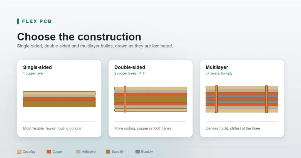
Three layer roles do the work in every construction on this page. The base film is the dielectric and the mechanical body of the part, almost always polyimide. The copper carries current, and its type and thickness decide how much bending the circuit tolerates. The coverlay is a second polymer film bonded over the conductors to insulate and protect them. Everything else — adhesive, stiffeners, surface finish — exists to support one of those three.
What the definition does not tell you is that a flex circuit is a mechanical part that happens to conduct. It has a fatigue life, a bend axis and a stiffness profile, and it is judged on those as much as on continuity. That is why the rest of this page is about decisions rather than characteristics.
Flex PCB vs Rigid, Rigid-Flex, FFC and Semi-Flex: Six Constructions Compared
The first question a buyer should answer is whether the part needs to be a flex PCB at all, and that question rarely gets asked. Flex is the right answer less often than its reputation suggests. Three of the five alternatives below exist specifically to beat it on cost, on assembly simplicity, or on both.
| Option | What it is | Best for | Fails when | Relative cost |
|---|---|---|---|---|
| Flex PCB | Copper on polyimide, coverlay both sides, no rigid sections | Tight envelopes, moving joints, weight and height limits, three-dimensional packaging | Component count or routing density climbs past what one or two layers carry; the part is large and static; nothing actually moves | Moderate |
| Flex with stiffener | A flex circuit with PI, FR4, stainless or aluminium bonded under selected areas | Connector tails, component areas, mounting points on an otherwise flexible part | The stiffener is specified as an afterthought, or placed against the bend | Moderate to high |
| Rigid-flex PCB | Rigid FR4 sections laminated into the flex stack, joined by flexible zones | Designs where connectors and cables are the reliability problem, or where the housing needs a hinge | The rigid sections could just have been separate boards and a cable; layer count is high; volume is low | Highest |
| FFC (flat-flex cable) | A conductor carrier: flat conductors in a film, terminated, no components | Point-to-point links, board-to-board jumpers, no impedance requirement, no components | Any component must be mounted, or the run needs controlled impedance or shielding | Lowest |
| Semi-flex (depth-routed FR4) | Standard FR4 routed thin along a line so it forms once | A bend that happens at installation and never again | The joint moves in service; the routed line is expected to survive repeated cycling | Low |
| Thin FR4 | Conventional rigid board, reduced thickness | A static installation where height is the only constraint | Anything at all moves, or the board is expected to flex during assembly | Lowest |
Four of those rows get confused with something they are not. Two of the confusions are expensive mistakes: treating a flat-flex cable as a flex PCB, and expecting a thin rigid board to flex.
Flex versus rigid-flex is a structural distinction rather than a quality hierarchy. A rigid-flex moves the rigid sections into the board itself, which removes the connectors, the cable assembly and the solder joints between them. That elimination is the entire saving, and it is the only defensible reason to pay rigid-flex prices. If your design still needs a connector at each end, you have paid for rigid-flex and kept the failure mode it was meant to remove. Where the mechanical design really does need a hinge, rigid-flex PCB construction is the right build.
Flex versus FFC is a cost decision most buyers never see. A flat-flex cable is a conductor carrier; a flex PCB is a circuit. If the run is point-to-point, carries no components and has no impedance requirement, an FFC does the same job for less money and with less design work. The case for a flex PCB starts when something must be mounted, when the geometry needs a shaped outline, or when the electrical performance is specified. This is worth raising at the quotation stage, because it is a design decision that has not yet been made.
Semi-flex is not flex. Depth-routed FR4 bends once and stays bent. It is right for a static installation, and wrong the moment the joint moves.
Thin FR4 is not flex either. It deflects under load, and because FR4 is brittle it eventually cracks. Expecting a thin rigid board to behave like a flex circuit is a false economy, and the failure arrives after the product has shipped.
Flex PCB Types: Single-Sided, Double-Sided and Multilayer
Flex PCB types are classified by copper layer count, and the count decides routing capacity, stiffness and price together.
Single-sided flex PCB
One copper layer, one side accessed, coverlay on both faces. It is the cheapest and the most flexible of the three, and it is the default for anything that moves. Its limit is routing: one layer means no crossings, so a design with more than a handful of nets cannot be laid out without jumping to double-sided.
Double-sided flex PCB
Two copper layers with plated through-holes between them. This roughly doubles routing capacity, and it changes the mechanics as well. Copper now sits on both sides of the neutral axis, so both foils carry strain through a bend. The inner foil is in compression rather than merely unstressed. The consequence is a stiffer part and a shorter fatigue life for the same geometry. How much shorter depends on the stackup and the bend, which is a calculation rather than a table, and it is worked out in the minimum bend radius calculation.
Multilayer flex PCB
Three or more copper layers, bonded with bondply or with adhesive, usually with plated through-holes through the whole stack. It is the densest and the stiffest construction, and layer count is the largest single lever on both price and bend performance. Above three layers, dynamic applications usually stop being a good fit and the design moves to flying leads or a rigid-flex transition.
What a flex stackup contains
A flex stackup is the ordered set of layers in the bend region, and it is the input every mechanical decision depends on. In its simplest form it is up to four layers plus an optional stiffener:
- Base film — the dielectric and the load-bearing body, almost always polyimide. Its thickness sets how far the outermost copper sits from the neutral axis.
- Adhesive, or none. An acrylic layer bonds copper to film in a conventional build; adhesiveless constructions bond directly. This choice changes total thickness without changing copper weight, which is why it changes bend performance.
- Copper — the conductors, specified by foil type (RA or ED) and weight. Foil type governs how much deformation the conductor tolerates before it cracks.
- Coverlay — a bonded film over the conductors, contributing its own thickness and stiffness. Openings in it are stress concentrators, so their placement is a design rule in its own right.
- Stiffener — a bonded FR4, polyimide, stainless or aluminium patch, present only where the part must behave rigidly. It is specified separately from the flexible section, and its edge position is a bend-zone constraint.
base film ─ adhesive ─ copper ─ coverlay
                                  ↑
                     stiffener added separately where needed
An adhesiveless build drops the adhesive line and bonds copper directly to the film. The stiffener is not part of the bend stack at all; it is added outside the bend region.
Naming the roles matters because each design rule acts on a different layer or on the stack as a whole. Bend radius responds to the entire stack, because strain depends on total thickness and on where the copper sits in it. Copper routing responds to the copper layer alone. Coverlay openings and stiffener edges are placement constraints on layers added after the circuit is routed. If you change any layer, you have changed the stackup, and the bend calculation has to be redone.
The allowable thickness for each role differs between a static build and a dynamic one. Those numbers are derived on the flex PCB bend radius page rather than tabulated here. A thickness table without the strain calculation that goes with it is the exact failure this cluster exists to correct.
Static and dynamic are different builds, not different specifications
A static flex is bent to install it and then fixed in place. A dynamic flex moves for its whole service life. These are not the same board with a different number written on the drawing. The copper type, the film thickness, the adhesive system and the permissible bend geometry all change. A part designed as static and installed in a moving assembly will fail. It will fail at the bend, which is the one place the design gave the least margin.
Flex PCB Materials: Polyimide, PET and the Adhesive Question
Flex PCB material selection is usually presented as a datasheet comparison, which is the wrong shape for the decision. Three substrate systems cover almost everything, and the choice between them turns on two questions: does the assembly see a soldering step, and does the part move?
| Attribute | PET (polyester) | Adhesive polyimide | Adhesiveless polyimide |
|---|---|---|---|
| Cost | Lowest | Moderate | Highest |
| Thickness for the same copper | Thinnest | Thickest — the adhesive adds to it | Thin |
| Survives reflow | No | Yes | Yes |
| Dimensional stability | Poor | Adequate | Best |
| Dissipation factor at 1 MHz | Not specified | 0.03 | 0.002 |
| Choose when | No soldering step, low service temperature, cost-dominated, static | Static or lightly dynamic, general purpose, cost-sensitive | Dynamic flex, fine features, loss-sensitive signals |
| Do not choose when | Any reflow or wave soldering, any elevated service temperature | Tight bend geometry, repeated motion, fine-line routing, controlled impedance | Cost is the binding constraint and the part is static |
PET is the cheapest of the three substrates and the thinnest. It also has the lowest service temperature, which is why it is disqualified more often than it is discussed. The disqualifier is what polyester is: PET is a thermoplastic, and its melting range sits near the peak temperatures a lead-free reflow profile reaches. A thermoset polyimide cures; a thermoplastic PET softens. A PET circuit therefore cannot go through a soldering oven, and if your assembly has any soldering step at all, the comparison above never needed to happen. That conclusion is not disputed. The exact temperature at which PET stops being suitable, however, circulates without a common primary source. Treat any figure you are given as a process window rather than as a material property.
The adhesive question is a thickness question in disguise. A conventional adhesive polyimide stack carries an acrylic layer between the copper and the base film. That adhesive adds thickness, and thickness is what bend geometry scales with. An adhesive construction is therefore a stiffer, less bendable part than an adhesiveless one at the same copper weight. Adhesiveless removes the layer: thinner for the same copper, better dimensional stability under temperature, and the better choice for anything that moves. The trade is straightforward — you pay for the thinner stack.
Thermal ratings need the same care as mechanical ones. Polyimide is routinely described as a 400 °C material, and that is the wrong number to design to. The manufacturer’s own page gives 400 °C as the upper end of the temperature range the film has been used in. It separately rates the same film with Underwriters Laboratories at a relative thermal index of 240 °C electrical and 200 °C mechanical (Qnity Electronics, Kapton HN, retrieved 2026-10-22). The RTI is the continuous-service figure; 400 °C is a peak. Treating a peak as a continuous rating is how a part passes qualification and fails in the field.
Copper type belongs in the material decision rather than in a separate topic. Rolled annealed (RA) foil is annealed into large, strongly aligned grains that resist fatigue cracking. Electrodeposited (ED) foil is grown, and its grain boundaries are where a bend starts a crack. In one foil maker’s repeated-fold test the rolled grades survived five to six cycles where an electrodeposited grade cracked on the second (JX Advanced Metals, retrieved 2026-10-22). One correction to the folklore: “ED is brittle” is too crude to act on, because foils made specifically for flex are engineered with coarser grains. RA remains the default for anything that moves, but the gap between good ED and RA is narrower than the popular summary implies. The deformation limits and what they mean for a radius are on the bend radius page, not repeated here.
A coverlay and a flexible solder mask are not interchangeable. A coverlay is a bonded polyimide film with routed or laser-cut openings, and it is a structural layer: it contributes thickness and stiffness, and it survives flexing. A flexible solder mask is a coating over the copper — a surface treatment. Both appear as options on a fabricator’s list and they do different jobs. In a bend zone, only the coverlay is a construction material. The film itself is covered in the polyimide base material properties guide.
The adhesive decision shows up in the electrical data too, and there it is not marginal. Dissipation factor at 1 MHz is 0.03 on the adhesive grade against 0.002 on the adhesiveless grade. That is a factor of fifteen, measured to the same method (Qnity Electronics, Pyralux AP and Pyralux FR, retrieved 2026-10-22).
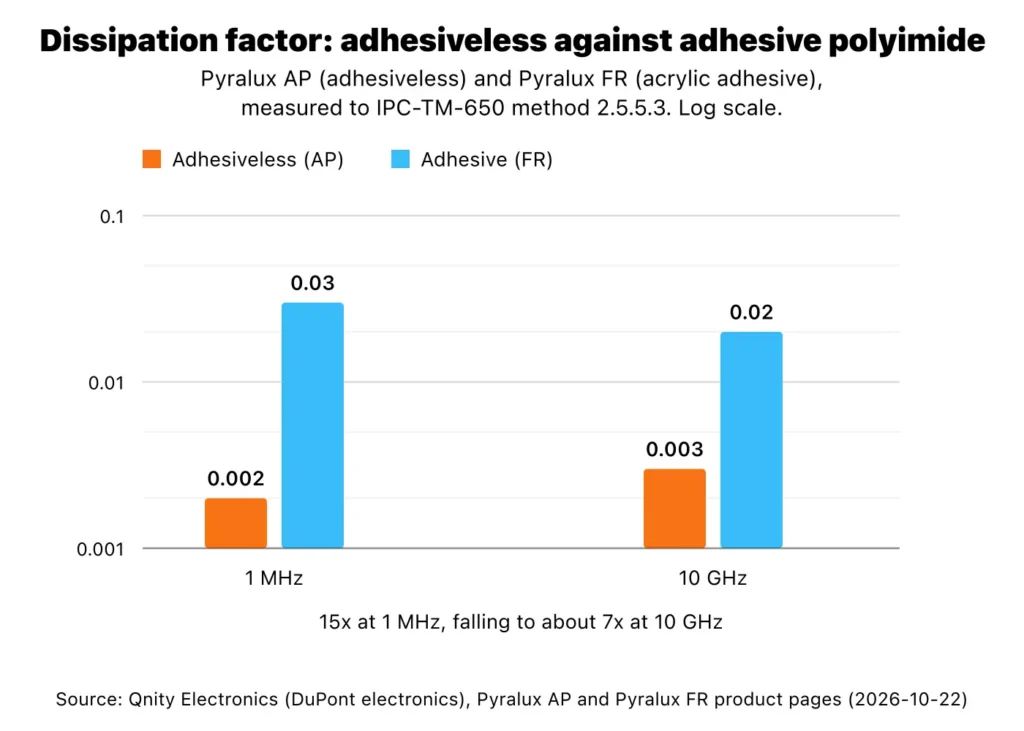
That is a loss argument before it is a thickness argument. If the run exceeds a few centimetres and carries a controlled-impedance signal, the acrylic layer is a lossy dielectric sitting directly in the field. Impedance design is its own discipline: see controlled impedance design, or size a trace directly with the impedance calculator.
The Design Rules That Decide Whether a Flex Circuit Survives
Five design rules carry most of the risk in a flex PCB. They are listed here in the order a layout hits them, at the depth needed to review a design — not to perform the calculation. Review them against the full DFM checklist for flex PCB before release.
1. Bend radius
Bend radius is the binding constraint on the whole design, and it is the one figure you cannot lift from a table. The radius your part needs depends on four things. Those are the total thickness of the flex stack at the bend, how many copper layers sit in it, where the copper sits relative to the neutral axis, and whether the bend is a one-time installation or repeated motion. The last of those alone can shift the requirement by an order of magnitude or more, depending on the source you read it from.
So this page does not quote a multiplier. The number is derived on flex PCB bend radius, which works it from the strain a copper foil can survive, using the deformation limits in IPC-2223, rather than from a published rule of thumb. Published rules of thumb are unusually loose here. Flex-to-install guidance and dynamic-flex guidance answer different questions and land in different ranges, and even within one duty cycle the denominators differ: some figures multiply total finished thickness, others a per-layer thickness. That spread is exactly why the derivation is worth doing.
2. Copper routing in the bend
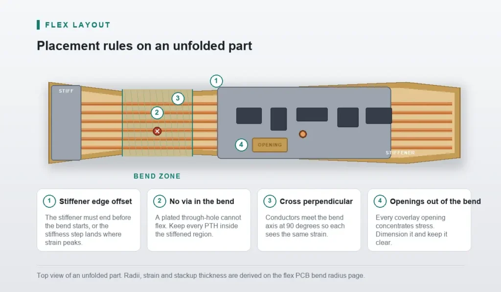
Conductors should cross a bend perpendicular to the bend axis, never parallel to it. A trace running along the bend direction accumulates strain over its whole length. A trace running across it is strained only over the width of the bend. Every conductor in the bundle then sees the same strain rather than a different amount each. Two related rules follow. Use a hatched or cross-hatched copper pour rather than a solid one in a bend zone, because solid copper bonded to the film resists the bend and delaminates. And keep plated through-holes out of the bend entirely, because a plated barrel cannot flex and will crack at the knee. Plated through-hole design covers the rest of the via rules.
3. Stiffeners
Stiffeners are required wherever the part is rigid by necessity: connector tails, component areas, mounting holes, and any point that takes an insertion force. Specify them as a separate item on the drawing — material, thickness, location and extent — rather than as a note. The failure to avoid is mechanical rather than dimensional. A stiffener edge that coincides with the start of the bend creates a stiffness discontinuity exactly where strain peaks, and the copper fatigues at that line. Move the stiffener edge back from the bend.
4. Coverlay openings
Every coverlay opening is a stress concentrator, because the film stops and the copper is exposed. Openings must be kept out of the bend zone and dimensioned on the fabrication drawing with their locations called out. IPC-2223 does not give a millimetre clearance for this; it prohibits flexing in an area where the covercoat is discontinuous. The margins fabricators quote are DFM practice built around that prohibition, not standard values, and they are worth respecting either way.
5. Panel, outline and bend geometry
Bend areas must not run out to a board edge, because the edge is a free boundary with nothing to carry the load and a tear starts there. Internal corners in or near a bend need a radius rather than a sharp angle, for the same reason. A sharp internal corner in a polyimide film propagates a crack across the part. Both are outline decisions, and both are cheap to fix at layout and impossible to fix at fabrication.
One scope note. Implantable and other safety-critical dynamic flex follows a separate qualification path with its own testing regime. Nothing on this page covers it.
What Drives Flex PCB Cost
Flex PCB cost is driven by five factors, and board area is a weaker predictor than buyers expect. Flex parts are small and oddly shaped. What a part costs is dominated by how efficiently it uses the panel and how many process steps its features add, not by how much laminate it contains.
The ranking below is our production observation across the parts we quote and build, not a benchmark study. There is no designed sample behind it, and no sample size is claimed: the order reflects the pattern our engineering team sees repeatedly rather than a measured result. Treat it as the start of a conversation about your part.
| Cost driver | Why it moves the price | How to reduce it |
|---|---|---|
| Panel utilisation | Flex parts are small and irregular. The share of a production panel they occupy is the strongest driver of unit price at volume, and a shape that nests badly wastes the panel | Nest or step-repeat the layout, review the outline against standard panel sizes, and accept an outline change that improves the yield per panel |
| Layer count | Every added layer is another lamination cycle, another bondply layer and another yield risk. It is the second-largest lever after panel utilisation, and the largest structural one | Route to the lowest layer count that carries the design, and check whether a double-sided build with a stiffener replaces a multilayer |
| Stiffener count and material | Each stiffener is a separate bonding step, and PI, FR4, stainless and aluminium are not priced alike | Use fewer, larger stiffeners instead of many small ones, and consolidate component areas onto one stiffened region |
| Coverlay opening count | Each opening is a routing or laser step, and each one is inspected | Consolidate openings; do not open the coverlay where a via can be tented instead |
| Test method | Electrical test is baseline. Bend-cycle or flex-life validation is a separate, priced activity | Decide up front whether the part needs flex-life validation, and say so in the enquiry rather than after the quote |
Flex cost drivers in rough order of effect, from our own quoted builds.
Two of those deserve a word on why they are counter-intuitive. Panel utilisation is routinely more important than board area, because the shapes that make a flex part a flex part are the shapes that nest badly. An outline with a tail and an ear wastes panel in a way a rectangle never does. The cheapest change is therefore sometimes to the outline rather than to the price. And layer count is not a linear cost, because each additional lamination cycle compounds the registration and yield exposure of the ones before it.
The comparison that matters is assembly cost against assembly cost. A flex or rigid-flex circuit removes connectors, cable assemblies, hand-soldered harnesses, and the labour and inspection that go with them. Comparing a flex board price against a rigid board price measures the wrong thing: the rigid assembly’s cost includes parts the flex version does not have. This is the only framing that survives a conversation with a finance team. It is also why a higher unit price can still be the cheaper design. Our flex PCB manufacturing capabilities set out what we build and to what tolerances.
And the honest counter-case: below a modest annual volume, and above a certain board area, a rigid board plus an FFC is cheaper in total than a flex circuit doing the same job. That is not a reason to avoid flex; it is a reason to ask the question before designing one. If nothing on the part moves and the run is point-to-point, the flex premium buys nothing.
How Flex PCBs Are Fabricated and Where Designs Fail
Flex PCB fabrication has five steps where a design decision becomes a failure, and each one has a rule that prevents it and a check that catches it. This is the part of the process a fabricator sees repeatedly, which a rule list alone does not convey. The question is not what the step is, but what it does to a marginal design.
| Process step | What can go wrong | Design rule that prevents it | How DFM review catches it |
|---|---|---|---|
| Material cutting and lamination | Polyimide and adhesive move during lamination, so features shift relative to the outline and registration error accumulates across the panel | Specify tolerances by feature class rather than one global tolerance, and dimension critical features from a datum that survives lamination | Stackup and datum review before CAM |
| Drilling and plated through-holes | A via in or near a bend, or outside the stiffened region, cracks at the barrel when the part flexes | Keep plated through-holes out of the bend zone and inside the stiffened area | Via-to-bend-zone and via-to-stiffener-edge checks |
| Coverlay lamination and opening | Adhesive squeezes out at an opening edge and the coverlay delaminates there; adhesive flow into a bend stiffens it unevenly | Keep openings out of the bend, dimension them, and allow for the adhesive fillet in the opening size | Coverlay-opening proximity review against the bend |
| Stiffener bonding | A stiffener edge that lands on the bend start puts a stiffness discontinuity where strain peaks, and the copper fatigues at that line | Offset the stiffener edge from the bend, and specify the offset on the drawing | Stiffener-to-bend clearance review |
| Surface finish and assembly | Polyimide absorbs moisture, and a part that has not been baked can blister or delaminate through reflow | Bake and fixture before assembly; specify the assembly method with the part | Assembly-method review at quotation |
The distinction worth holding on to is between a rule and a reason. “Keep the stiffener away from the bend” is a rule, and it is easy to violate because nothing about it looks wrong on a drawing. A stiffener edge on the bend start creates a stiffness step at the point of maximum strain, so the copper fatigues at that line is a reason. That is what lets you judge a case the rule does not cover.
The same applies to moisture. Polyimide is hygroscopic, which is why a flex assembly is a separate capability rather than an afterthought. The part has to be dried and fixtured, and the handling between baking and reflow matters. A design that is correct on paper can still fail at assembly if nobody specified that step. Our quality and testing capabilities cover what is inspected and how.
Note what the table is and is not. The failure chain is production observation from our own process: the steps where these faults actually appear on our line, and the checks that catch them. It is drawn from the same body of quoted and built work as the cost ranking, with the same absence of a designed sample. It is not a quotation from a standard, and no standard publishes it in this form. That distinction is the honest one to make about a fabricator’s process knowledge. It is also why the chain is useful: it describes what happens on a line, not what a design guide thinks should happen.
How to Specify a Flex PCB for Quote
Send these ten items and the first response is usually a quote. Leave out the first four and the first response is a question, which is a round trip you did not need.
- Board outline and bend locations, drawn in the installed shape, not the flat shape.
- The stackup, with total flex thickness stated for the bend region specifically.
- Bend radius and bend diameter, each with a tolerance.
- Static or dynamic. For dynamic, the target cycle count and the motion the part sees.
- Copper type and weight — RA or ED, and the foil thickness.
- Coverlay type and opening locations.
- Stiffener material, thickness and location, dimensioned as a separate item.
- Connector part number and mating drawing, plus contact side, pitch, insertion length and required tail thickness.
- Surface finish, and any impedance requirement with its tolerance.
- Assembly requirement, including whether a fixture is needed.
A quote built without items 1 to 4 is a guess dressed as a price. Those four determine whether the part can be built at all. The gap between a guess and a quote is exactly the round trip this list removes. Send those details with your enquiry and the review starts at the layout.
Frequently Asked Questions
Are flex PCBs more expensive than rigid PCBs?
Per part, usually yes, sometimes by a large multiple. Per assembly, often no. A flex circuit can remove connectors, a cable assembly and the labour and inspection that go with them. The comparison that matters is therefore total assembly cost against total assembly cost. The flex premium is only worth paying when it removes something.
What are the disadvantages of flex PCBs?
Components can only be mounted on stiffened, non-bending areas, so density is lower than on a rigid board of the same area. Copper weight and layer count are limited compared with rigid boards. Assembly needs fixtures and moisture control. And the design rules are stricter: a marginal layout that would pass on FR4 will fail at the bend.
What is the difference between a flex PCB and a rigid-flex PCB?
A flex PCB is flexible over its whole area. A rigid-flex laminates rigid FR4 sections into the same board, joined by flexible zones, so the rigid and flexible parts are one continuous circuit. Rigid-flex removes the connectors and solder joints between board and cable, which is the only reason to pay for it.
Can a flex PCB be used for repeated bending?
Yes, but only a construction designed for it. Static and dynamic flex are different builds: the copper type, film thickness and adhesive system all change. A static part installed where it moves will fail at the bend. The allowable geometry for dynamic service is derived on the flex PCB bend radius page.
What is the difference between FPC and FFC?
An FPC is a flexible printed circuit: copper on a film substrate, with components and a designed circuit. An FFC is a flat-flex cable: a conductor carrier, usually point-to-point, with no components. If your run has nothing to mount and no impedance requirement, an FFC is normally the cheaper correct answer.
What is the minimum order quantity for flex PCBs?
It depends on the construction and the tooling involved, and it is quoted per project rather than published as a single figure. Prototype quantities are routinely possible; the economics improve sharply with panel utilisation, so the figure is quoted per project against your actual requirement.
Conclusion
Choose the construction first, the material second, and specify the bend properly or nothing else matters. Most flex problems trace back to one of those three being decided by default rather than deliberately.
That is also the order a fabricator works in. If you send the installed shape, the stackup and the static-or-dynamic answer with the enquiry, the review starts at the layout instead of at the missing information. Request a flex PCB quote and we will review the stackup before you commit.
Sources
- IPC / Global Electronics Association, IPC-2223F: Sectional Design Standard for Flexible/Rigid-Flexible Printed Boards, for the design rules on bend geometry, covercoat discontinuities and stiffener placement referenced in the design-rules section, and for the copper deformation limits that the linked bend-radius page derives from. Revision status is tracked at the publisher’s standards status page.
- IPC / Global Electronics Association, IPC-6013F: Qualification and Performance Specification for Flexible/Rigid-Flexible Printed Boards, for the acceptance requirements a flex build is qualified against.
- IPC / Global Electronics Association, IPC-4202C: Specification for Flexible Base Dielectrics for use in Flexible Printed Boards, IPC-4203C: Cover and Bonding Material for Flexible Printed Circuitry, and IPC-4204C: Flexible Metal-Clad Dielectrics for Use in Fabrication of Flexible Printed Boards, for the base film, coverlay and laminate specifications.
- IPC / Global Electronics Association, IPC-A-600M: Acceptability of Printed Boards, for the visual acceptance criteria referenced in DFM review.
- IPC, IPC-TM-650: Methods of Test for Printed Circuit Boards, cited by individual method rather than by manual revision: method 2.5.5.3 for the dielectric constant and dissipation factor values, and method 2.4.18.1 for copper foil elongation.
- Qnity Electronics (DuPont electronics), Pyralux AP flexible circuit laminate and Pyralux FR flame-retardant laminate, for the dielectric constant and dissipation factor values at 1 MHz and 10 GHz and their test methods. Retrieved 2026-10-22. DuPont’s flexible-circuit and polyimide pages now redirect to Qnity, the electronics business spun out of DuPont.
- Qnity Electronics, Kapton HN polyimide film, for the UL relative thermal index ratings and the stated temperature range of use. Retrieved 2026-10-22.
- JX Advanced Metals, HA rolled copper foil for flexible printed circuits, for grain orientation, modulus and folding-endurance data by foil type. Retrieved 2026-10-22.