LED PCB design connects an LED package, its electrical supply, its optical surroundings and a path for removing heat. A useful layout begins with the actual LED and operating conditions, then carries those choices into the board files and assembly instructions. The result may use FR-4, aluminum or another construction, depending on the application.
The decisions are linked. Moving LEDs closer together may change light distribution and local heating; changing the supply may change the available driver headroom. Set the requirements before drawing the final footprint or ordering a board.
Punti Chiave
- Use the selected LED’s package documentation to check the land pattern, polarity and any thermal-pad electrical connection.
- Design the current path around the chosen supply and driver. Parallel LED strings do not necessarily share current equally.
- Assess heat flow through the complete mounted assembly; an aluminum board alone does not establish an acceptable LED junction temperature.
- Give the fabricator and assembler the design files, component orientation, cooling assumptions and agreed test requirements together.
Start with LED PCB design requirements
Write down the conditions the board must meet before selecting its substrate or LED spacing. A board inside a sealed luminaire has different optical and cooling constraints from an exposed indicator board.
| Input | What to define |
|---|---|
| Application and light | Required output, color, illuminated area, uniformity and the position of any lens or diffuser. |
| LED and drive | LED manufacturer and order code, current target, supply range, and whether the driver is on or off the board. |
| Operating environment | Expected ambient temperatures, enclosure, airflow, duty cycle and nearby heat sources. |
| Mechanical assembly | Board outline, mounting points, connectors, available cooling surface and electrical isolation needs. |
| Produzione | Quantity, assembly scope, file format, inspection and test requirements agreed with the supplier. |
Keep assumptions with their sources. An enclosure temperature estimated at the start is not a measured board temperature, and a preliminary diffuser position is not proof of uniform illumination.
Choose the LED footprint and check polarity
Start with the exact LED order code and its current package documentation. Use its recommended land pattern and check the pad dimensions, solder mask, stencil and component orientation against the assembler’s process. A package name alone is not a reliable substitute for the part-specific drawing.
Identify anode and cathode on both the library footprint and assembly drawing. Add a clear polarity or reference mark where it will remain visible after assembly, and check the connector polarity in the same review. The separate guide to identifying LED polarity explains common marking methods.
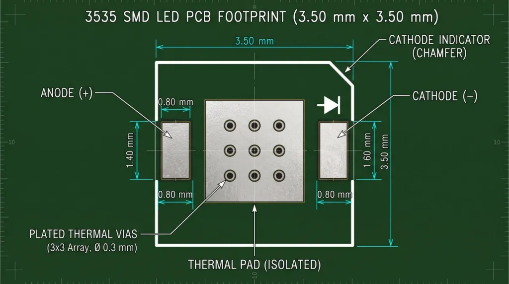
If the package has a thermal pad, verify whether it is electrically isolated, connected to a terminal or subject to another manufacturer requirement. Do not assume the pad may be connected to chassis or ground. Where vias sit in a solderable pad, discuss their construction with the fabricator and assembler: solder can wick into an open via and affect the joint. Cree’s XLamp thermal-design note discusses that issue for the isolated-pad packages in its scope; another LED must be checked on its own terms.
Plan LED current distribution and the driver handoff
Choose a drive arrangement that controls or limits current under the intended supply and temperature conditions. Depending on the application, that may mean a constant-current driver, an appropriate resistor arrangement or a driver supplied as part of another assembly. Check the selected LED and driver documentation rather than assuming every board needs the same circuit.
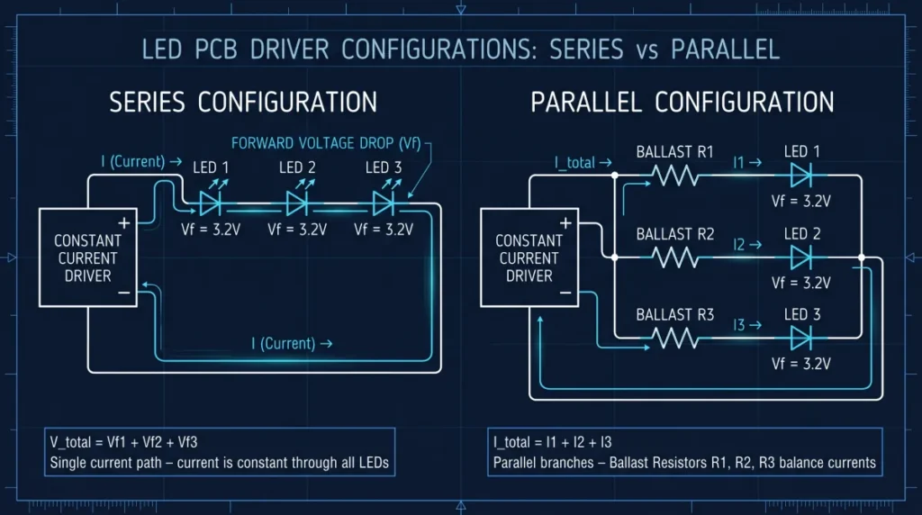
For LEDs in series, the same string current flows through each device. Check that the combined forward voltage at the intended current and temperature, plus wiring loss, fits the driver’s specified output-voltage range. Separately verify the minimum supply and headroom required by that driver topology; a stated output range may already include the driver’s own headroom. Forward voltage varies between parts and with operating conditions, so a typical value alone does not establish the worst case.
For parallel strings, small differences in forward voltage can make one branch carry more current than another. Separate current regulation or suitably designed individual ballast resistors can address the imbalance, but resistor tolerance, voltage drop, power loss and temperature still need review. Analog Devices’ parallel-string example explains why independent string regulation can be useful.
Size copper paths for the actual current, temperature rise, copper construction and manufacturing capabilities. Document the supply range, current target, connector pinout, polarity and driver location in the handoff. Mains-connected designs also require an appropriate electrical-safety and isolation review.
Set LED spacing around the optical goal
Place LEDs for the complete optical assembly, not for a bare board viewed on a desk. LED beam pattern, viewing direction, diffuser material, diffuser height and the illuminated area’s edges all affect the result.
Start with a proposed arrangement and the optical requirement: for example, a maximum acceptable brightness variation across a panel. Keep LEDs and connectors clear of mounting hardware, consider shadows from the enclosure, and check whether nearby heat sources create local hot spots. Closer spacing may improve overlap in one assembly while increasing local heat concentration.
In its light-shaping diffuser guidance, Luminit discusses LED divergence, source spacing and the distance to the diffuser when addressing visible LED sources. Its examples apply to its own films and specified source geometry, not every optical assembly.
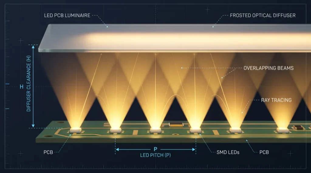
There is no universal LED-to-LED spacing. Use optical modelling where suitable, then inspect or measure a representative prototype with the intended LEDs, current, enclosure and diffuser. Record what was tested; a change to any of those parts can require another check.
Plan thermal management and the complete heat path
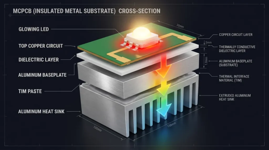
Follow heat from the LED junction through its package and solder joint into the board, then through the mounting interface and any chassis or heat sink to the environment. The weak point may be the mounting interface or enclosure rather than the board material alone.
Copper near the LED can spread heat; thermal vias or a different board construction may help transfer it elsewhere. Their value depends on the package, layer stack and final assembly. In application note AN052, ams OSRAM identifies LED placement, thermal losses, nearby heat sources, cooling and the heat-sink interface as PCB-level inputs.
FR-4 and aluminum are design choices, not interchangeable guarantees. FR-4 may suit a lower-power design or a board with an adequate copper-and-via heat path. An insulated aluminum construction can move heat toward a metal base, but its dielectric, mounting interface and heat sink remain part of the path. Special direct-thermal-path constructions need separate electrical-isolation and manufacturing review. See aluminum PCB thermal design for stackup and a worked thermal budget.
Check the selected LED’s junction-temperature limits and measurement method. A datasheet thermal-resistance value is tied to its stated test conditions; do not treat it as a measured value for the finished assembly. Compare calculations or simulations with tests at representative current, ambient temperature, mounting pressure and duty cycle. The PCB thermal hotspot analysis guide covers ways to investigate a hot area.
Flexible LED boards need their own material, mounting and heat-flow review. For their construction and mechanical context, see the flex PCB overview.
Prepare the LED PCB assembly and fabrication handoff
A release package should explain the decisions behind the files as well as the finished geometry. The supplier can then check the board construction and component placement against the intended use, rather than guessing from a Gerber image.
| Input | Decisione | Source or assumption | Verification and status | Handoff |
|---|---|---|---|---|
| LED and package | Exact order code, footprint and orientation. | Selected LED datasheet and package drawing. | Compare the land pattern, polarity and pad connection; record whether checked. | BOM, placement data and assembly drawing. |
| Optical assembly | LED positions, lens or diffuser and target coverage. | Illumination target and diffuser or enclosure drawing. | Review the model or measure a representative assembly; record the test status. | Placement drawing, mechanical references and optical acceptance target. |
| Supply and current | Supply range, driver location, current and string arrangement. | Supply specification and LED and driver datasheets. | Check compliance, tolerances, polarity and limits; record any open checks. | Schematic, connector pinout and operating requirements. |
| Heat path | Board construction, local copper, mounting interface and cooling. | Component limits and stated mounting and ambient assumptions. | Compare analysis and representative temperature tests; distinguish calculated from measured. | Stackup, mounting drawing, thermal assumptions and test conditions. |
| Mechanical fit | Outline, holes, keepouts and connector clearances. | Enclosure and mounting drawings. | Check the board against the enclosure and assembly process; record fit-test status. | Board outline, drill data and mechanical drawing. |
| Release package | Revision, quantities, assembly scope and acceptance criteria. | Agreed file revision and supplier requirements. | Match designators and revisions; record whether the package is approved for release. | Board files, BOM, placement data, drawings and test instructions. |
Ask the supplier which board-file format and tolerances it accepts, and whether the proposed material, finish and assembly process can be combined. The guide to Gerber, BOM, CPL and stackup files explains the purpose of each file in more detail.
Preliminary LED PCB layout example
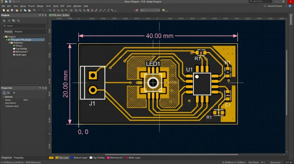
Considera un ipotetico low-voltage indicator board. Its preliminary inputs are a 40 × 20 mm board, a 5–6 V supply, one white LED and a 70 mA current target. These are teaching assumptions, not measured results or recommended dimensions for every product.
With the lower-left corner as the origin, place the LED center at approximately x = 20 mm and y = 10 mm. Reserve space near one edge for the supply connector and between it and the LED for the driver; check the actual component outlines and keepouts before positioning them. A preliminary FR-4 heat path could run from the LED solder pads into copper, through the board and an interface to a metal enclosure. The board, interface, electrical isolation and mounting must be assessed together; that proposed path is not proof of adequate cooling.
| Voce | Starting point | Check before release |
|---|---|---|
| LED | Cree JE2835 3-V R Class, for example order code JE2835AWT-R-H40GA0000-N0000001. | Confirm availability, package drawing, polarity, land pattern and operating limits for the exact order code. |
| Fattore | TPS92612-Q1, with the current-setting network designed for the 70 mA target. | Check current tolerance, startup, faults, voltage compliance and dissipation in the actual circuit. |
| Layout | One emitter centered at x = 20 mm, y = 10 mm; connector and driver areas remain preliminary. | Check the actual optical opening, mechanical fit, copper paths and assembly access. |
| Raffreddamento | A preliminary FR-4-to-metal-enclosure heat path; interface and mounting details remain open. | Assess the complete heat path and measure a representative mounted prototype. |
Il Cree datasheet lists a 2.95 V typical and 3.1 V maximum forward voltage for this LED class at 150 mA and 25 °C. Those figures do not establish the worst-case forward voltage at the example’s 70 mA over its intended temperature range. That missing value must be checked before approving the circuit.
At a 70 mA setting, TI’s driver electrical table lists 0.4 V maximum supply-to-output dropout, including the sense voltage. The table’s general conditions are a 5–40 V supply and a driver junction temperature of −40 to 150 °C. Assuming a 5.0 V minimum at the driver’s supply pins, subtracting that 0.4 V leaves 4.6 V for the LED and downstream wiring under those conditions. If 5.0 V is specified at a remote supply, account for the upstream lead loss first and check that the voltage at the driver still meets the table conditions. This is a preliminary voltage budget, not proof of compliance: the LED’s worst-case forward voltage at the actual current and temperature, downstream wiring losses and current-setting tolerance still need to fit. Check startup, faults and the driver’s own power dissipation as well. The cited LED figure at 150 mA and 25 °C is not a substitute for those checks.
For an initial power allowance only, assume the LED has a 3.0 V forward drop at 70 mA: its electrical input would be approximately 0.21 W. The assumed voltage is not a guaranteed datasheet value at that operating point. The number is neither a measured junction temperature nor the driver loss, and it does not prove the chosen board and mounting can remove the heat. Update the calculation with component-specific limits and test the assembled product.
The handoff would identify the LED order code, intended current, connector polarity, preliminary board outline and cooling assumptions in the worksheet, BOM, placement file and drawings. It would also flag the open electrical and thermal checks rather than presenting them as passed.
Common LED PCB design mistakes
- Copying a similar-looking footprint. Check the exact package drawing, polarity and thermal-pad connection before releasing the library part.
- Assuming parallel strings share current. Review each branch’s regulation or ballast design, tolerances and power dissipation.
- Setting spacing without the optical assembly. Test the LED arrangement with the actual diffuser, enclosure and operating current.
- Treating the substrate as the whole cooling system. Include mounting contact, nearby heat sources and the heat sink or enclosure in the thermal assessment.
LED PCB design questions
Must an LED PCB use aluminum?
No. FR-4, aluminum and other constructions can all be used for LED boards. The choice depends on heat generation, the package, cooling and mounting, electrical needs, mechanical constraints and the supplier’s available construction.
How is LED current controlled?
A suitable driver or current-limiting arrangement controls current within the selected LED’s operating limits. The design must account for supply variation, LED forward-voltage variation, temperature and tolerances rather than relying on a nominal voltage alone.
Is there a universal spacing between LEDs?
No. Placement depends on the LED’s light distribution, the required illuminated area, diffuser and enclosure geometry, and thermal conditions. Model or test the actual assembly against its uniformity target.
From layout to production
Before release, reconcile the LED part and polarity, current and voltage checks, optical layout, heat path and file revisions. For a discussion of fabrication and assembly requirements, share those decisions with the LED PCB manufacturing team.