Blog
Qui puoi acquisire conoscenze professionali che coprono l'intera catena, dalla progettazione PCB all'assemblaggio, oltre a un'analisi precisa delle ultime tendenze nel settore elettronico.
Industrial PCB Production: Process & QA
Industrial PCB production turns an approved circuit-board design into bare boards and, when ordered, populated assemblies for industrial equipment. The route includes fabrication, component assembly, inspection and agreed testing. Approval depends on the specified build, operating conditions and acceptance criteria. A motor controller, sensor interface and cabinet-mounted control board can require different materials, mechanical support…
PCB in alluminio: progettazione termica e materiali
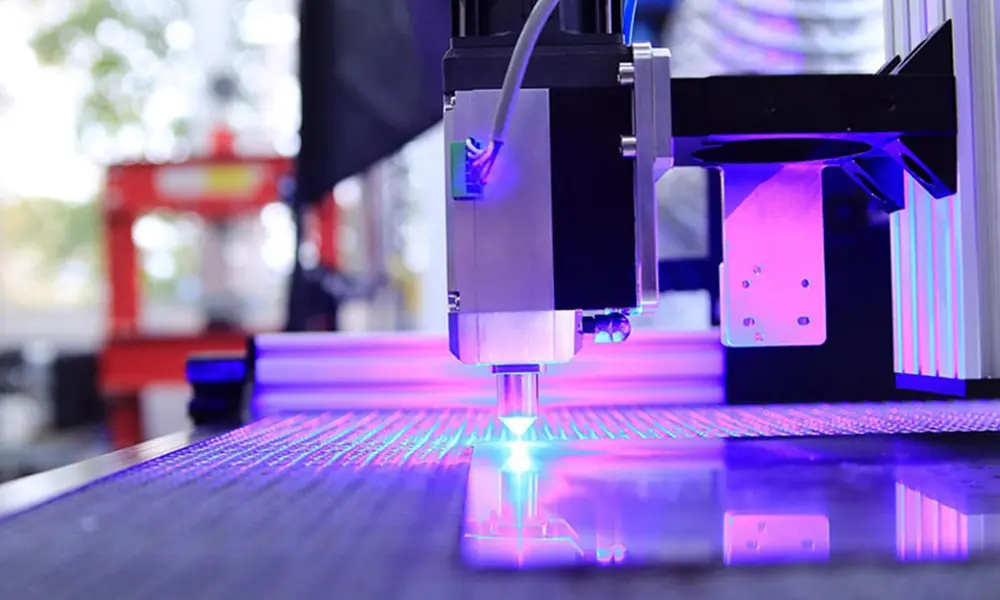
An aluminum PCB is a printed circuit board that combines copper circuitry, an electrically insulating thermal dielectric and an aluminum base. The dielectric carries heat toward the metal while separating the circuit electrically. This construction is useful for LED lighting and power electronics when the board, mounting interface and cooling surface form a suitable heat…
PCB HDI: stackup, microvie e progettazione
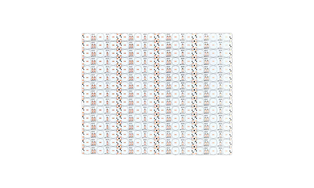
An HDI PCB, or high-density interconnect printed circuit board, uses fine conductors and compact interlayer connections to fit more wiring into a given area. Laser-drilled microvias and thin buildup layers help connect dense component pads without using a full-thickness hole at every connection. The design question is whether those features solve a routing constraint worth…

PCB rigido: materiali, costruzione e scelte progettuali
A rigid PCB, or rigid printed circuit board, supports components and connects them through copper conductors on a substrate designed to retain its shape in service. It suits electronics whose circuitry stays fixed within an enclosure, rather than bending during use. Choosing one means matching its construction to the circuit, mounting, connectors and environment. Layer…

PCB flessibile: tipi, materiali, stackup e regole di progettazione
A flex PCB is a circuit built on a flexible polymer film, usually polyimide, with copper conductors bonded to it and a coverlay protecting them. That is the definition, and it is the part already answered above the search results. It is not the part that decides whether your build works. Four questions decide that,…
Raggio di curvatura dei PCB flessibili: come calcolarlo e specificarlo
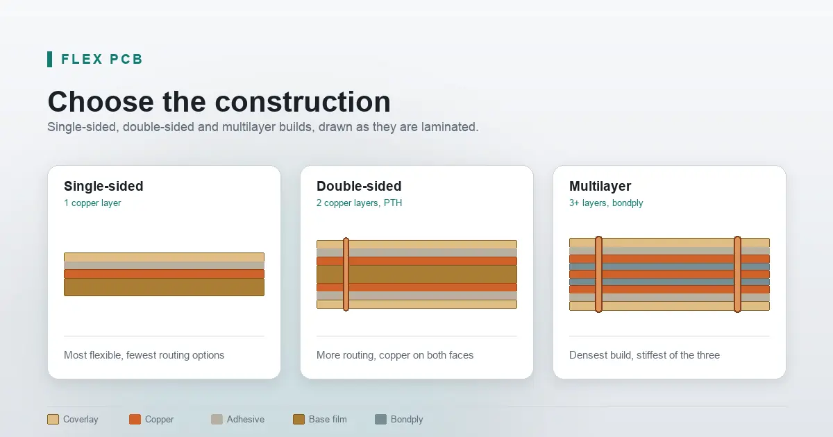
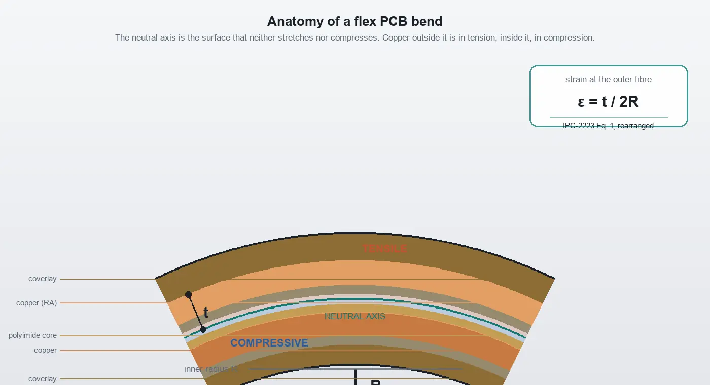
You have a stackup, a housing envelope, and a mechanical engineer asking for a flex PCB bend radius. The answer is not a lookup table; it is a strain calculation, and the multipliers in the tables are what that calculation returns once you fix a stackup. Every published multiplier, whether it reads 6×, 10×, 12×,…
Guida alla saldatura a rifusione: processo, profilo e difetti
Reflow soldering is the process that attaches surface-mount components to a printed circuit board by heating stencilled solder paste until it melts, wets the component terminations and forms the joint on cooling. It is the primary assembly method for almost every modern electronic product, and it is the step where the most expensive mistakes become…
Che cos’è l’ ispezione delle Paste Solder (SPI)? Misurazioni, difetti e controllo di qualità
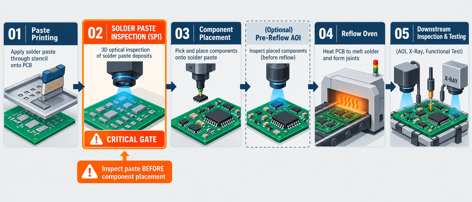
Solder paste inspection (SPI) checks paste deposited on a PCB after printing and before component placement. A 3D SPI system measures deposit volume, height, area, and alignment against programmed limits. It allows defective prints to be held and corrected before placement and reflow. For hardware engineers and PCBA buyers, the key decision is whether the…
I 10 migliori software per la progettazione di PCB nel 2026
KiCad is the strongest free desktop starting point for engineers choosing PCB design software in 2026. Altium Designer through Altium Develop is a strong paid choice for small teams that want shared libraries, browser review, and electrical–mechanical collaboration in one connected workflow. Both support serious board design; the purchasing decision is whether the surrounding workflow…
Guida ai resistori SMD: codici, dimensioni, footprint e limiti
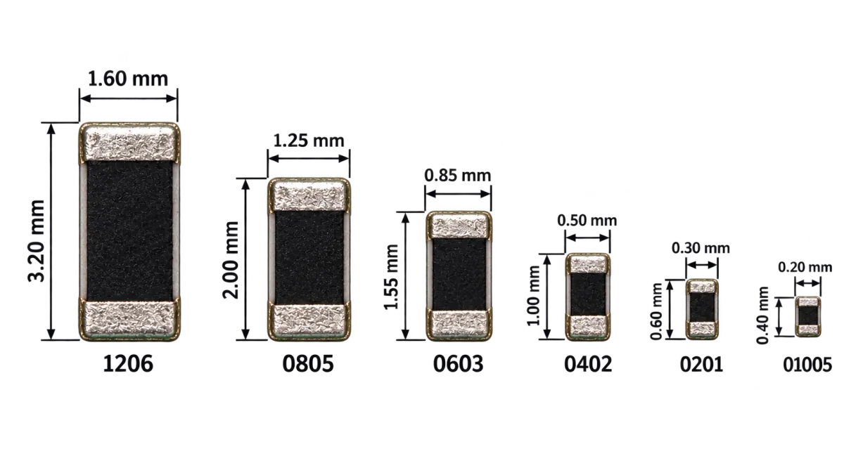
An SMD resistor is a fixed-value resistor in a leadless rectangular package that solders to pads on the surface of a printed circuit board rather than passing through holes. It is typically the most numerous component on a board, and the one most often specified from habit rather than from the datasheet. Most guides to…
Laminato rivestito di rame (CCL): tipi, produzione, prestazioni e standard
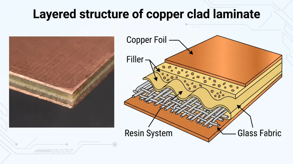
Copper clad laminate, or CCL, is a base material from which PCB conductors are formed. It consists of copper foil bonded to an insulating material such as cured glass-reinforced epoxy, a flexible polymer film, or a thermally conductive dielectric on a metal base. In a conventional multilayer rigid PCB, patterned CCL commonly becomes a core.…
JLCPCB vs PCBWay: quale produttore di PCB è adatto al tuo progetto? (2026)
For a straightforward PCB prototype or a small assembly order that fits JLCPCB’s Economic PCBA rules, start with JLCPCB, especially when the components are already in its inventory. For rigid-flex or extensive custom fabrication requirements, shortlist PCBWay early. These recommendations follow from JLCPCB’s economical assembly tier and PCBWay’s documented advanced manufacturing options. The JLCPCB vs…

What Is GND? Meaning, Types, and PCB Grounding Explained
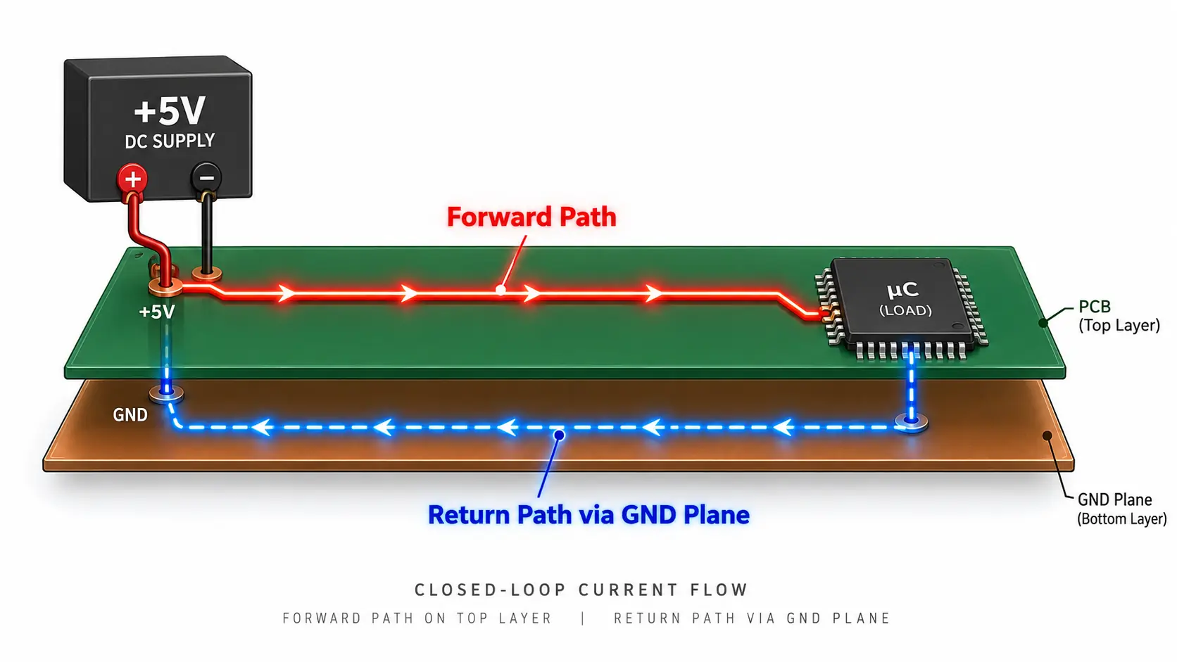
GND appears on almost every circuit diagram, PCB, power supply, and electronic module. It is often described as “zero volts” or “the negative terminal,” but neither description is universally correct. In electronics, GND stands for ground. It is the reference node against which other voltages are measured and, in many circuits, part of the path…
What Is a Through Hole? PCB Types, Uses, and Design Guide
A through hole is an opening that passes completely from one side of a printed circuit board (PCB) to the other. It may be plated with conductive copper to create an electrical connection, or left unplated for mechanical use. Through holes are commonly used for component leads, connectors, vias, mounting hardware, alignment pins, and slots.…

Cosa sono i package QFN? Una guida pratica per la progettazione e l'assemblaggio di PCB
I pacchetti QFN compaiono in tutto, dagli alimentatori e moduli wireless a sensori, microcontrollori ed elettronica automobilistica. La loro impronta ridotta, i percorsi elettrici brevi e il trasferimento di calore efficiente li rendono un'alternativa interessante ai pacchetti con terminali più grandi. Tuttavia, le stesse connessioni inferiori che risparmiano spazio rendono anche il design dell'impronta QFN, la saldatura e l'ispezione meno tolleranti. Quindi,…

Guida ai Materiali per PCB: Tipi, Proprietà e Selezione
Il materiale del PCB influisce su molto più che la resistenza fisica di un circuito stampato. Esso incide su impedenza, perdita di segnale, dissipazione del calore, stabilità dimensionale, affidabilità dell'assemblaggio, producibilità, tempi di consegna e costi. Un materiale che funziona bene per un controller di base potrebbe fallire in un modulo radar a 77 GHz, in una scheda LED ad alta corrente o in un dispositivo medico rigido-flessibile.…

Progettazione PCB a impedenza controllata: stackup, specifiche e test
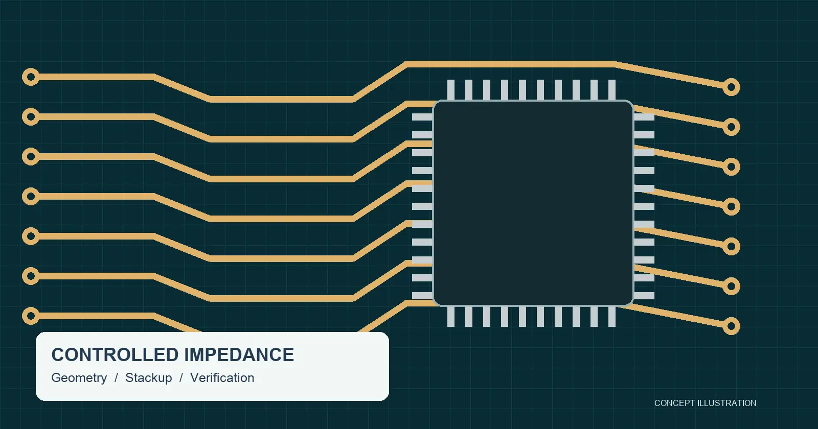
Controlled impedance is the practice of designing and manufacturing PCB traces so their characteristic impedance meets a specified target and tolerance. The result depends on the conductor geometry, dielectric construction, and reference planes. A complete requirement also states how the manufacturer will verify the finished structure. A note that says only “50 ohms” leaves important…
Resistore da 10k: Codice Colore, Usi e Come Scegliere Quello Giusto
Un resistore da 10k è un componente elettrico passivo con una resistenza nominale di 10.000 ohm (10kΩ). Nel design circuitale moderno, è uno dei valori più onnipresenti trovati sia su breadboard che su PCB di produzione. Ingegneri e hobbisti si rivolgono ai resistori da 10k perché rappresentano un punto di equilibrio elettrico ideale: limitano la corrente a livelli sicuri,…

Progettazione di antenne PCB: layout, materiali e produzione
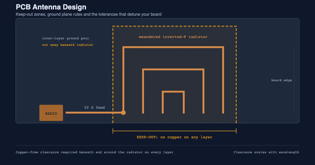
A PCB antenna is a copper trace or pattern etched directly onto a printed circuit board that transmits and receives radio frequency electromagnetic waves. It is the cheapest way to give a product wireless connectivity, because it adds no connector, no cable and no bill-of-materials line. It is also the part of a design most…
Anodo e Catodo LED: Come Identificare i Terminali Positivi e Negativi
Un LED (Diodo a Emissione di Luce) è un dispositivo semiconduttore polarizzato che consente il passaggio di corrente in una sola direzione. Per illuminare un LED, è necessario collegare correttamente i suoi terminali positivo e negativo all'interno del circuito. Nei LED standard a foro passante, il terminale più lungo e il lato arrotondato rappresentano l'anodo, mentre il terminale più corto e il…