A rigid-flex PCB combines rigid circuit regions and flexible circuit layers in one construction. The rigid regions support components and can contain additional conductive layers, while the flexible region connects them through the enclosure. Conductors cross each rigid-to-flex transition to carry signals and power between regions.
Consider a hypothetical compact device with a populated control region and a populated interface region on different sides of an internal enclosure corner. A flexible connection must route around that corner. For this example, the flex is bent during installation and remains stationary during normal operation; service handling still needs consideration. A rigid-flex design is one option alongside separate rigid boards with a cable and a flex circuit with local stiffeners.
Principais conclusões
- Compare packaging, connections, assembly, service and validation before choosing rigid-flex over a cable or stiffened flex.
- Define the rigid and flex stackups together. A passive stiffener supports a flex circuit but does not add integrated rigid circuit layers.
- Route conductors through transitions, while placing the actual bend and stress-sensitive features away from those interfaces using fabricator-approved clearances.
- Specify how the assembly bends and is handled. Repeated movement calls for qualification under representative conditions, with agreed electrical pass/fail criteria.
- Compare the complete assembly cost and send the fabricator the regional construction, mechanical constraints and test requirements for a useful quote.
When does a rigid-flex PCB make sense?
Rigid-flex is worth evaluating when connecting populated regions inside an enclosure creates a difficult packaging or assembly problem. For the hypothetical device, each of the three architectures changes where connections, assembly work and validation occur.
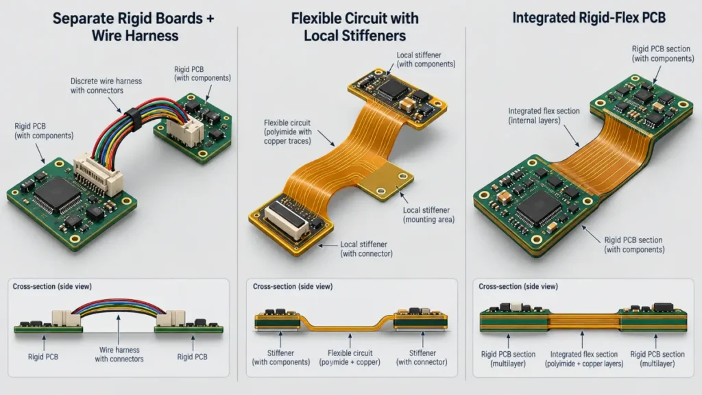
| Architecture | Packaging and connections | Service and verification |
|---|---|---|
| Rigid boards and cable | Boards link by cable; connectors need mating space. | Boards may be replaceable separately; check the cable path and contacts. |
| Stiffened flex | Continuous flex links supported component areas. | The circuit may need replacement as a unit; check joints and flex. |
| Rígida-flexível | Flex links rigid circuit regions; it can remove their cable and connectors. | The assembly may need replacement as a unit; check transitions and connections. |
Separate rigid boards can be designed independently, but the cable must be routed and mated during assembly. Replacing a board separately depends on connector access. Check connector retention and service access as well as the cable path and electrical contacts. The guide to rigid PCB construction covers the board side of this option.
Stiffened flex can connect locally supported component areas without an internal board-to-board cable. Passive stiffeners do not add electrically integrated rigid-board copper layers. Component assembly can require support fixtures; check enclosure fit, supported-area assembly, solder joints and flex behavior.
Rigid-flex integrates flexible circuitry with rigid regions that have their own conductive layers. The single assembly needs a coordinated stackup and manufacturing process. Check interlayer connections, transitions, mechanical fit and assembly access.
None of these choices wins for every device. A removable cable may be valuable for repair; integrated rigid-flex may be useful when the cable and mating space are difficult to accommodate. Cusack Electronics’ rigid-flex guide discusses construction and the distinction from stiffened flex. The broader guide to flex PCB types and design choices covers other flex configurations.
For the rest of the example, assume the team selects rigid-flex because the enclosure makes the internal cable and connectors awkward. That is a design hypothesis to check with a mechanical model, prototypes and supplier quotes, not a demonstrated saving.
How is a rigid-flex PCB stackup built?
A rigid-flex stackup defines which materials and conductive layers exist in each region and how they connect. A design might use a polyimide-based flexible circuit with copper conductors that continues into both rigid areas. The rigid areas can add glass-reinforced epoxy material such as FR-4 and further copper layers; plated connections in the rigid regions can connect those layers to the flex circuitry.
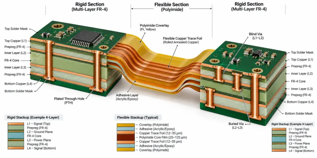
The exposed flexible span needs its own defined construction. A coverlay can protect copper on a flex surface, with openings where the design needs access; adhesives or bonding layers may also be part of the build. Layer order, materials and bonding choices depend on the design and fabricator. A rigid-to-flex transition is the interface where the rigid construction ends and the flexible span continues.
For the device, propose the flexible conductors needed between control and interface regions, identify the extra copper needed within each rigid region, and show where the relevant connections change layers. Ask the fabricator to review the complete regional stackup before treating it as buildable.
Design the transition and flexible region
Route through the rigid-to-flex transition
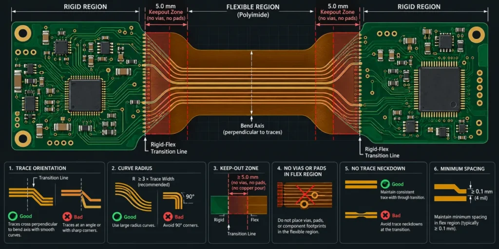
Traces must cross the transition to connect the rigid and flexible regions. Route them smoothly through the interface and avoid abrupt direction or width changes there. Where appropriate, route conductors across a bend approximately perpendicular to its axis; check the actual bend geometry and electrical routing needs before fixing the orientation.
Place pads, vias, plated holes and abrupt neckdowns away from transitions and active bend areas using clearances approved for the proposed construction. All Flex’s rigid-flex guidance recommends waiting until traces have exited the rigid area and cleared the keepout margin before necking them down, and advises against placing vias close to the boundary. Put the intended bend within the flexible span, away from the rigid interfaces, subject to the fabricator’s review. The clearance depends on the stackup and use, so a generic fixed keepout is not a substitute for an agreed drawing.
In the hypothetical enclosure, the conductors leave the control region, continue through the flex around the corner and enter the interface region. Show both transition boundaries and the intended bend on the drawing. Check that the available straight portions and enclosure clearance allow the bend to occur where planned, without pinching the flex or placing it against a sharp feature.
Define the bend and the motion
Mark the bend axis, the line about which the flex curves, as well as the bend location, direction and installed geometry. Check the design in three dimensions with the enclosure and assembly sequence. Include expected tolerances, any contact with the housing, and the path the flex takes while the product is opened or serviced.
The example is intended to stay bent during normal operation. That differs from a flex that moves repeatedly during use, although installation and repair can still impose movement. Copper choice, layer construction, fit and the resulting strain all need review for the actual motion. Sierra Circuits’ flex design guidelines discuss routing and bending considerations. For bend calculations and numerical examples, use the separate flex PCB bend-radius guide.
Specify materials and the regional stackup
Give the fabricator enough information to review both electrical and mechanical requirements, rather than assuming a standard rigid-board stackup will work throughout the assembly.
- Layer construction: Identify the layers present in each rigid area and in the flex, their order, intended materials, copper specifications, coverlay, openings and any bonding layers. Define the region boundaries and proposed interlayer connections.
- Copper and motion: Describe the intended bend and ask the fabricator to review copper type, thickness, processing and orientation for that use. The appropriate choice depends on the finished construction as well as the motion.
- Electrical behavior: Show signal and return paths across the transition. Where needed, specify impedance, spacing and electrical performance targets for the relevant regions and ask how the stackup change will be evaluated.
- Environment and assembly: State the temperatures, moisture, chemicals or other conditions the device must tolerate, along with relevant assembly and service constraints. Material selection is also covered in the PCB material guide.
For the example, the proposed flex must fit the corner while still carrying the required control-to-interface connections. If the required routing changes the flex construction, revisit both the mechanical fit and electrical performance before releasing the design.
How manufacturing and assembly affect the design
Rigid-flex fabrication requires the rigid and flexible regions to align and bond as intended. All Flex’s manufacturing overview discusses sequential lamination, alignment, resin flow and coverlay. The actual process sequence depends on the proposed build, so review the stackup and drawings with the fabricator early.
Ask how the supplier plans to form and protect the flex region, maintain alignment and inspect the rigid-to-flex interfaces. Discuss panelization, tooling and the support needed to handle the circuit through fabrication and assembly. A carrier or fixture may be needed to support the assembly while components are placed and soldered.
For the compact device, check whether components, inspection points and possible rework sites remain accessible on both rigid regions. Also check how an operator installs the circuit without forcing the flex against the enclosure. If either region is difficult to inspect or repair after folding, that can affect the architecture decision as well as the assembly plan.
What drives rigid-flex PCB cost?
Rigid-flex cost depends on the construction and the work required to build and verify it. Regional layer counts, material choices, lamination, alignment, cutouts, panel utilization, yield, inspection and order quantity can all affect a quote. A complex single piece can also affect the cost of scrap or replacement when one region is defective.
For the hypothetical device, compare the same categories across all three architectures:
- Bare circuits and interconnects: Compare fabrication of the separate boards, stiffened flex or rigid-flex assembly, along with any cables and connectors each design actually needs.
- Assembly and test: Include connector mating where applicable, fixtures, handling, inspection and electrical or mechanical qualification.
- Service: Consider access and whether a failed region can be replaced separately or requires a larger assembly to be replaced.
Removing the internal cable and connectors changes the parts and operations to be quoted; it does not establish that rigid-flex has the lowest total assembly cost. Request comparable quotes using the same quantities, acceptance criteria and service assumptions.
Test the design before production
Electrical tests, mechanical fit checks and flex qualification answer different questions. Agree on the samples, methods and acceptance criteria before using their results to release the design.
- Electrical connectivity and isolation: Define the nets to test and their continuity and isolation acceptance criteria. Include the connections between rigid regions and the conductors that cross the flex.
- Construction and transition inspection: Agree on how to inspect the region boundaries, coverlay and relevant fabrication features. Specify any additional inspection or representative cross-sectioning needed for the build.
- Fit and handling: Install a representative assembly in the enclosure. Check the bend location, contact points, component access and the assembly and service motions expected for the device.
- Repeated flexing, if applicable: Define the actual operating motion and qualify a representative circuit or custom coupon. Agree on bend geometry, direction, movement rate, a cycle target based on expected lifetime bends, environment, sample plan and electrical pass/fail limits, including when electrical measurements are taken. Ensure the test construction and routing represent the features under evaluation; check the assembled product separately where needed.
The example’s intended stationary use calls for fit and handling checks. If a later revision places the flex in a moving hinge, add a representative dynamic test for that motion. An October 2025 PCEA Flexperts discussion of flex testing notes that flex life qualification is almost always a custom test and that its cycle count should exceed the expected number of bends over the product’s lifetime. A passing continuity check at one point in time does not establish bend life, and a coupon result must be interpreted in light of how well it represents the finished design and use.
IPC announced the IPC-6013F qualification and performance standard revision. Agree with the fabricator on the applicable standards, editions, class and any project-specific acceptance criteria. A statement of IPC compliance alone does not prove the circuit will survive the device’s particular motion for its intended life; flex life needs qualification for the application.
What should you send a rigid-flex PCB manufacturer?
Send a fabrication package that explains the assembly in its flat and installed states. For the hypothetical device, identify the control and interface regions and show how the flex travels between them. Include:
- Fabrication files and a drawing with board outlines, layer mapping, drill data, region boundaries and the relevant dimensions and tolerances.
- Proposed rigid and flex stackups, copper and material requirements, coverlay openings, finishes and the intended interlayer connections.
- Bend axis, direction, location and required installed geometry; state whether movement occurs during installation, service or repeated operation.
- Enclosure and assembly constraints, including clearances, component access and any useful mechanical model. Provide assembly information if assembly is in scope.
- Operating environment and, for repeated movement, the motion, cycle target and qualification conditions.
- Prototype and production quantities, schedule, requested standards and editions, class, and electrical, inspection and mechanical test acceptance criteria.
Ask the fabricator to confirm the proposed construction, capabilities, transition and bend clearances, test approach and any assumptions before final release. Resolve differences between the flat drawing and the installed model before relying on the quote.
Rigid-flex PCB FAQs
Is stiffened flex the same as rigid-flex?
No. A stiffener mechanically supports part of a flex circuit but does not itself add electrically integrated rigid PCB layers. Rigid-flex combines flexible circuitry with rigid circuit regions in one construction. The two options can serve similar packaging needs, so compare their component support, assembly and service requirements for the actual device.
Can a rigid-flex circuit be designed for repeated movement?
Yes, but suitability depends on its construction and the motion it must survive. Specify the operating geometry and environment, then agree on representative dynamic testing, a cycle target and electrical pass/fail criteria. A circuit intended to stay bent after installation needs a different use description from one that moves throughout service.
For the compact-device example, the next decision is whether the proposed regional stackup and installed geometry can be built and verified within the assembly’s constraints. When those requirements are ready, use the rigid-flex PCB manufacturing page to request a fabrication quote.