An SMD resistor is a fixed-value resistor in a leadless rectangular package that solders to pads on the surface of a printed circuit board rather than passing through holes. It is typically the most numerous component on a board, and the one most often specified from habit rather than from the datasheet.
Most guides to these parts stop at two questions: what size is it, and what does the code mean. Both matter, and both are answered below. But they are not the questions that get a design into trouble. A chip resistor’s published power rating is not the power it can dissipate in your product. Its package code is not a power rating at all. And the pad dimensions underneath it decide whether it solders reliably, which no package table tells you.
This guide covers the four decoding systems, a sourced package and voltage table, thermal derating with a worked calculation, land pattern geometry, and how package size changes what an assembly line can actually place and inspect.
Key Takeaways
- A chip resistor’s published wattage applies at 70 °C ambient and derates linearly to zero at the part’s upper category temperature. A 0603 rated 0.1 W is not a 0.1 W part inside a hot enclosure.
- The four-digit package code is a footprint in hundredths of an inch, not a power rating. Power belongs to the series and the manufacturer, which is why two datasheets can both be right and still print different numbers for a 1206.
- Voltage rating is a separate limit from power, and on small packages it usually binds first. A high-value 0402 can fail on voltage while dissipating a small fraction of its rated watts.
- Below 0603, package size stops being an electrical decision and becomes a process decision. It sets what your assembly house can place, inspect and rework.
- Use the largest package the layout allows. 0603 is the practical default: cheap, easy to inspect, and hand-reworkable.
What Is an SMD Resistor?
An SMD resistor is a fixed-value resistor in a leadless rectangular package, soldered to pads on the surface of a printed circuit board rather than through holes.
Four layers make up nearly every chip resistor. A ceramic substrate carries the part mechanically. A resistive film on top of it sets the resistance value. Metal terminations at each end make the electrical connection to the board. A protective overcoat seals the film against moisture and handling.
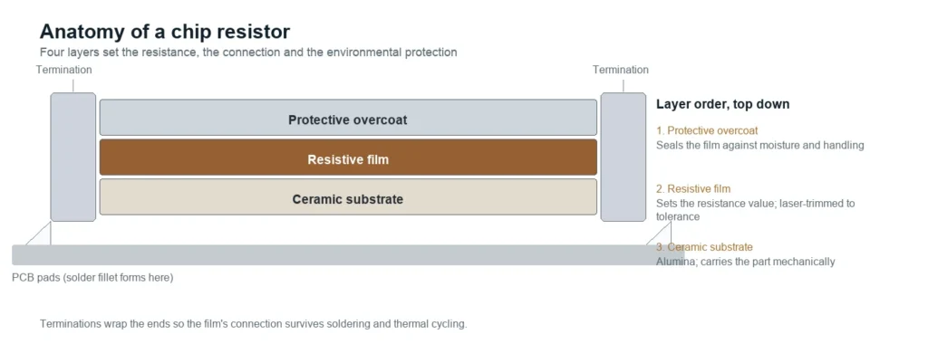
SMD resistors displaced leaded parts for three practical reasons: no holes need drilling, both sides of the board become usable, and pick-and-place machines handle parts far smaller than a human can. The same package family covers capacitors, LEDs and diodes, which is why a board full of identical-looking rectangles is difficult to read by eye.
This guide is written for designers specifying parts, technicians identifying them, and engineers checking a BOM before a build.
How to Read SMD Resistor Codes
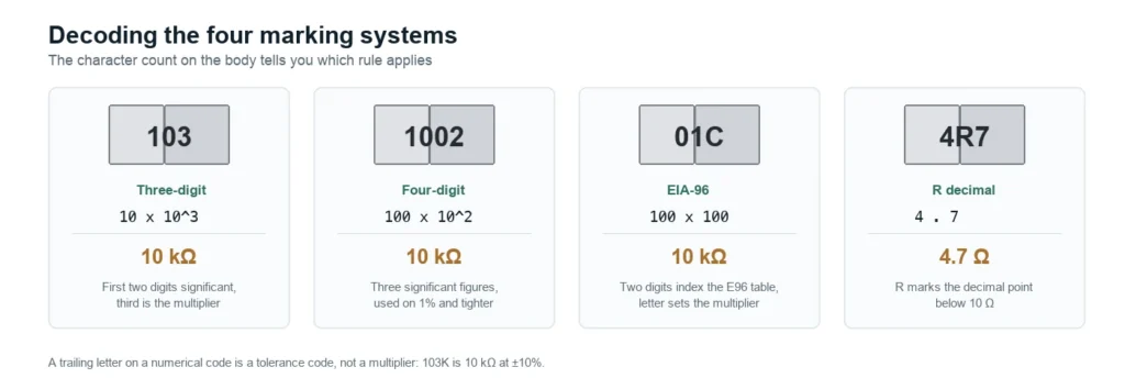
Four marking systems cover practically every chip resistor, and the one that applies is decided by how many characters are printed on the body. Read the character count first, then apply the matching rule.
The Three-Digit Code
The first two digits are the significant figures and the third is the power-of-ten multiplier. A marking of 103 is 10 × 10³, or 10 kΩ. 472 is 47 × 10², or 4.7 kΩ.
| Code | Significant figures | Multiplier | Value |
|---|---|---|---|
| 100 | 10 | ×10⁰ | 10 Ω |
| 220 | 22 | ×10⁰ | 22 Ω |
| 472 | 47 | ×10² | 4.7 kΩ |
| 103 | 10 | ×10³ | 10 kΩ |
| 104 | 10 | ×10⁴ | 100 kΩ |
| 105 | 10 | ×10⁵ | 1 MΩ |
A three-digit code implies E24 values and typically ±5% or ±1% tolerance.
The Four-Digit Code
Three significant figures plus a multiplier, used on ±1% and tighter parts. 1002 is 100 × 10², or 10 kΩ — the same value as 103, expressed with more precision. 4992 is 499 × 10², or 49.9 kΩ.
The EIA-96 Code
Two digits select a value from the 96-entry E96 table, and one letter sets the multiplier. This system is used on 1% parts where there is no room for four digits.
The multiplier letters, which two independent references give identically (EEPower, Resistor SMD Code; SparkFun, Decoding Resistor Markings, both retrieved 2026-10-21):
| Letter | Multiplier | Letter | Multiplier | Letter | Multiplier |
|---|---|---|---|---|---|
| Z | 0.001 | A | 1 | D | 1,000 |
| Y or R | 0.01 | B or H | 10 | E | 10,000 |
| X or S | 0.1 | C | 100 | F | 100,000 |
Two worked examples: 01C is code 01 = 100, multiplier C = 100, giving 10 kΩ. 92Z is code 92 = 887, multiplier Z = 0.001, giving 0.887 Ω.
The 96 codes and the values they index, from the IEC 60063 standard series table (Vishay, Standard series values in a decade for resistances and capacitances, E3 to E192 according to IEC 60063, document 28372, retrieved 2026-10-21):
| Code → value | Code → value | Code → value | Code → value | Code → value | Code → value | Code → value | Code → value |
|---|---|---|---|---|---|---|---|
| 01 → 100 | 02 → 102 | 03 → 105 | 04 → 107 | 05 → 110 | 06 → 113 | 07 → 115 | 08 → 118 |
| 09 → 121 | 10 → 124 | 11 → 127 | 12 → 130 | 13 → 133 | 14 → 137 | 15 → 140 | 16 → 143 |
| 17 → 147 | 18 → 150 | 19 → 154 | 20 → 158 | 21 → 162 | 22 → 165 | 23 → 169 | 24 → 174 |
| 25 → 178 | 26 → 182 | 27 → 187 | 28 → 191 | 29 → 196 | 30 → 200 | 31 → 205 | 32 → 210 |
| 33 → 215 | 34 → 221 | 35 → 226 | 36 → 232 | 37 → 237 | 38 → 243 | 39 → 249 | 40 → 255 |
| 41 → 261 | 42 → 267 | 43 → 274 | 44 → 280 | 45 → 287 | 46 → 294 | 47 → 301 | 48 → 309 |
| 49 → 316 | 50 → 324 | 51 → 332 | 52 → 340 | 53 → 348 | 54 → 357 | 55 → 365 | 56 → 374 |
| 57 → 383 | 58 → 392 | 59 → 402 | 60 → 412 | 61 → 422 | 62 → 432 | 63 → 442 | 64 → 453 |
| 65 → 464 | 66 → 475 | 67 → 487 | 68 → 499 | 69 → 511 | 70 → 523 | 71 → 536 | 72 → 549 |
| 73 → 562 | 74 → 576 | 75 → 590 | 76 → 604 | 77 → 619 | 78 → 634 | 79 → 649 | 80 → 665 |
| 81 → 681 | 82 → 698 | 83 → 715 | 84 → 732 | 85 → 750 | 86 → 768 | 87 → 787 | 88 → 806 |
| 89 → 825 | 90 → 845 | 91 → 866 | 92 → 887 | 93 → 909 | 94 → 931 | 95 → 953 | 96 → 976 |
Note that R appears in this system and in the decimal-point system below, so a marking containing R is not automatically an EIA-96 code.
The “R” Decimal Point and Tolerance Letters
For values below 10 Ω, R marks the decimal position: 4R7 is 4.7 Ω, 0R5 is 0.5 Ω, 0R01 is 0.01 Ω.
One correction worth making explicitly, because it is taught the wrong way round on some component sites: on a chip resistor, a trailing letter is a tolerance code, not a multiplier. In a marking like 103K, the value comes from the digits alone — 103 is 10 kΩ — and K indicates ±10% tolerance. The letter adds information about the part; it does not change the arithmetic.
Marking conventions are not fully standardised. EEPower’s guide states this directly, noting that a manufacturer may use a variation or something entirely different, so the datasheet governs over any chart.
SMD Resistor Sizes and Package Codes
The four-digit code is the footprint in hundredths of an inch, and it is not a power rating.
Power and voltage columns below are for the Yageo RC series, a general-purpose thick-film range (retrieved 2026-10-21); other series and vendors differ, sometimes substantially — Vishay’s CRCW e3 rates its 2010 and 2512 at 400 V and 500 V, well above the 200 V shown here.
| Imperial | Metric | Size (in) | Size (mm) | Typical power | Typical max voltage | Typical use |
|---|---|---|---|---|---|---|
| 01005 | 0402 | 0.016 × 0.008 | 0.4 × 0.2 | 1/32 W | 15 V | Wearables, SiP |
| 0201 | 0603 | 0.024 × 0.012 | 0.6 × 0.3 | 1/20 W | 15–25 V | Smartphones |
| 0402 | 1005 | 0.040 × 0.020 | 1.0 × 0.5 | 1/16 W | 50 V | High-density boards |
| 0603 | 1608 | 0.060 × 0.030 | 1.6 × 0.8 | 1/10 W | 50–75 V | General purpose |
| 0805 | 2012 | 0.080 × 0.050 | 2.0 × 1.25 | 1/8 W | 100–150 V | Hand-assembly friendly |
| 1206 | 3216 | 0.120 × 0.060 | 3.2 × 1.6 | 1/4 W | 200 V | Higher dissipation |
| 1210 | 3225 | 0.120 × 0.100 | 3.2 × 2.5 | 1/2 W | 200 V | Power paths |
| 2010 | 5025 | 0.200 × 0.100 | 5.0 × 2.5 | 3/4 W | 200 V | Power electronics |
| 2512 | 6332 | 0.250 × 0.120 | 6.3 × 3.2 | 1 W | 200 V | Power, current sense |
Why published dimensions disagree. The imperial code is nominal in inches and the metric code is nominal in millimetres, and the two do not convert exactly. A 0603 is 0.060 × 0.030 in, which is 1.52 × 0.76 mm, while its metric equivalent 1608 is 1.6 × 0.8 mm. Published dimensions also carry a manufacturing tolerance. Two datasheets can both be correct and still print different numbers for the same package, which is why Vishay’s thin-film MCT 0603 datasheet gives the body as 1.55 × 0.85 mm (Vishay, document 28700, retrieved 2026-10-21) while its own thick-film CRCW e3 document uses 1.6 × 0.8 mm.
Why power ratings disagree, and why it matters more. Power rating belongs to the series, the film technology and the manufacturer — not to the package code. A general-purpose 1206 thick-film part is commonly rated 1/4 W, and a 1206 from a high-power series can be rated 1/2 W. Treating the package code as a power rating is the error this section exists to prevent, and it leads directly into the next one.
Power Rating and Thermal Derating
A chip resistor’s published power rating is not the power it can dissipate in your product. It is the power it can dissipate at a stated ambient temperature, and it falls to zero before the part reaches its upper category temperature.
Vishay’s precision thick-film chip resistor data sheet defines rated dissipation P₇₀ as the maximum permitted load at 70 °C ambient, and gives the derating endpoints directly: 100% of rated power at 70 °C, falling linearly to 0% at 155 °C (Vishay, D/CRCW e3 standard thick film chip resistors, document 20035, retrieved 2026-10-21). The same document specifies a permissible film temperature of 155 °C and calls out EN 60115-1 as the governing generic specification for its test procedures.
That linear rule is the whole calculation. Between 70 °C and 155 °C, usable power is:
usable fraction = (155 − ambient) ÷ 85
So at 100 °C, a part retains (155 − 100) ÷ 85 ≈ 65% of its rated power. At 125 °C it retains about 35%. Below 70 °C the rating is generally not increased.
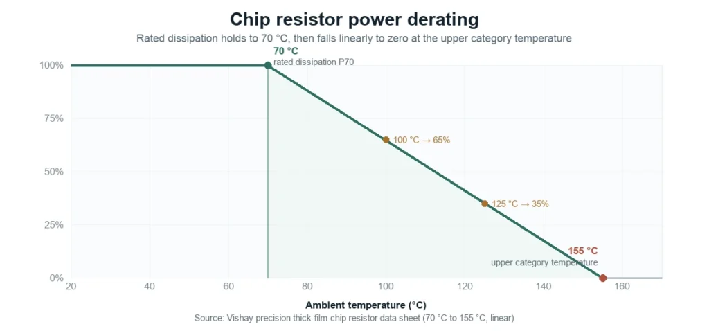
Worked example. A 0603 rated 0.1 W sits in an enclosure that reaches 100 °C. Available power is 0.1 W × 0.65 = 65 mW. The circuit puts 9 mA through a 1 kΩ part: P = I²R = 0.009² × 1,000 = 81 mW.
The part fails — and this is the trap: at 70 °C the same 81 mW would have sat comfortably inside the 100 mW rating. The part passes on the bench and fails in the enclosure.
Why small packages are hit hardest. Power density rises as the body shrinks, and there is less pad copper to sink heat into. The pad and its copper are part of the thermal path, which is why the land pattern in the next section is also a thermal decision, not only a mechanical one.
Mitigations, in the order worth trying: move up a package size, widen the pads and the copper connecting to them, add thermal vias where the layout allows, or split the dissipation across two parts in series or parallel.
Land Patterns and Pad Geometry
The pad dimensions decide whether the part solders reliably, and they are not the same as the component dimensions.
The pad is deliberately larger than the termination. That extra copper gives solder somewhere to wet, and it gives the part self-alignment: surface tension in the molten solder pulls a slightly misplaced chip into position during reflow.
Three dimensions govern the result. Pad width sets joint strength. Pad length — the extension beyond the termination — sets the fillet and the self-alignment force. The gap between the two pads sets bridging risk and decides how much solder sits between the terminations.
IPC-7351 defines three density levels. Level A gives the most land protrusion and the widest process window, and suits low-density boards and wave soldering. Level B is the nominal default and is what most production boards use. Level C gives the least protrusion for high-density designs, and IPC-7351 calls for user qualification before adopting it.
Vishay’s land pattern document states that its figures reflect IPC-7351 and IEC 61188-6-2, and it publishes a set for each (Vishay, recommended solder pad dimensions for surface-mount resistors and fuses, document 28950, retrieved 2026-10-21). In both, C is the gap between the two pads, Y is the pad length along the component axis and X is the pad width across it, so the overall footprint is Z = C + 2Y:
| Package | IPC-7351, reflow (C, Y, X, Z) | IEC 61188-6-2, reflow (C, Y, X, Z) |
|---|---|---|
| 0201 | 0.27, 0.43, 0.42, 1.13 | 0.30, 0.24, 0.32, 0.78 |
| 0402 | 0.40, 0.55, 0.60, 1.50 | 0.55, 0.35, 0.55, 1.25 |
| 0603 | 0.70, 0.90, 1.00, 2.50 | 0.90, 0.55, 0.90, 2.00 |
| 0805 | 1.00, 0.90, 1.45, 2.80 | 1.10, 0.65, 1.30, 2.40 |
| 1206 | 1.75, 1.15, 1.80, 4.05 | 2.10, 0.80, 1.65, 3.70 |
| 1210 | 1.75, 1.15, 2.65, 4.05 | 2.10, 0.80, 2.50, 3.70 |
Read the 0603 row as two pads 1.00 mm wide and 0.90 mm long, separated by a 0.70 mm gap, giving a 2.50 mm overall footprint. The overall dimension is the useful check: the pad must be wider than the body it carries and the footprint longer than the part, which is why Z = C + 2Y holds on every row above.
The IEC set is consistently tighter — a smaller pad on a wider gap — and the two standards are not interchangeable. IPC-7351’s three density levels adjust these further; the table above is the nominal reflow set for Vishay’s thin-film chip parts, and a different series or vendor will publish different numbers.
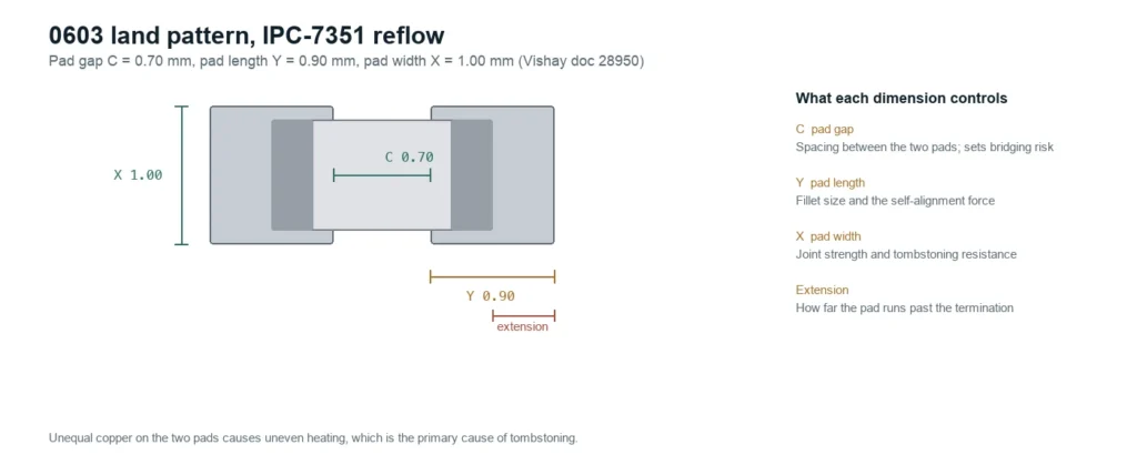
Two further points belong here. Pads are defined as solder-mask-defined or non-solder-mask-defined, and the stencil aperture is usually reduced from the pad to control paste volume. And unequal copper on the two pads of a small chip means unequal heating, which is the primary mechanism behind tombstoning — picked up again in the assembly section.
Voltage Rating and Other Limits
A chip resistor carries two independent limits — a power limit and a voltage limit — and on small packages the voltage limit usually binds first.
Power rating is a thermal property. Voltage rating is a dielectric property, set by the body length and the spacing between terminations. They are physically unrelated, and both must be satisfied.
The crossover is where the binding constraint flips. A resistor reaches its rated voltage at V = √(P × R), so the critical resistance where voltage takes over from power is R = V² ÷ P. For a 0402 rated 50 V and 1/16 W, that is 50² ÷ 0.0625 = 40 kΩ. Above 40 kΩ the part is voltage-limited and can break down while dissipating a small fraction of its rated watts. For a 0603 rated 75 V and 0.1 W the crossover is about 56 kΩ, and for a 1206 rated 200 V and 1/4 W it is about 160 kΩ.
Typical maximum working voltages for general-purpose thick-film series run roughly 50 V for 0402, 50–75 V for 0603 and 100–150 V for 0805. From 1206 upward they sit at 200 V (Yageo, RC series general-purpose thick film chip resistors, retrieved 2026-10-21). Two caveats matter: voltage does not keep rising with size — Yageo’s RC series holds 200 V from 1206 all the way to 2512 — and there is real brand-to-brand spread, with Vishay’s CRCW e3 rating its 2010 and 2512 at 400 V and 500 V and some vendors rating 0402 at 25 V rather than 50 V. Check the exact series.
Two more boundaries are worth knowing. Short-term overload voltage is a separate and higher specification; Vishay’s CRCW-HP e3 datasheet, for example, rates its parts for a pulse load well above the continuous operating voltage (Vishay, document 20043, retrieved 2026-10-21). And pulse handling differs from continuous rating: standard thick film handles pulses relatively poorly, which is why anti-surge and pulse-withstanding series exist.
Tolerance, TCR and Value Series
Tolerance tells you how far a part can sit from its marked value the moment you buy it. TCR tells you how far it will move afterwards. They are different specifications, bought separately.
| Tolerance | Typical film technology | Typical use |
|---|---|---|
| ±5% | Thick film | Pull-ups, LED limiting, non-critical dividers |
| ±1% | Thick or thin film | General precision, feedback networks |
| ±0.5% | Thin film | Precision dividers, references |
| ±0.1% and tighter | Thin film, metal foil | Instrumentation, calibration |
The E-series link is the part most guides omit: which values you can actually buy depends on the tolerance. E24 pairs with ±5% and E48 with ±2%. E96 pairs with ±1%, and E192 with ±0.5% and tighter (Vishay, Standard series values in a decade for resistances and capacitances, E3 to E192 according to IEC 60063, document 28372, retrieved 2026-10-21). The value spacing within each series mirrors the tolerance it supports, so specifying a non-E96 value at ±1% means a non-standard part, a longer lead time and a higher price.
TCR, in ppm/°C, is where thick and thin film separate most sharply. A buyer’s guide to resistor specifications puts thick film at roughly ±100 to ±200 ppm/°C and thin film at roughly ±5 to ±25 ppm/°C — close to an order of magnitude (Abacus Select, Resistor Types & Specs, retrieved 2026-10-21). TCR matters in precision dividers, current-sense paths and reference circuits. It does not matter for a pull-up or an LED limiter.
Tolerance and stability are also not the same thing. Tolerance is initial accuracy at purchase; long-term stability is how far the value drifts in service. A tight-tolerance part can still drift, and the two are specified separately on the datasheet.
What Are the Different Types of SMD Resistor?
The type is set by how the resistive element is made, and that construction decides the precision, noise and power handling you can have — usually not all three at once.
Tolerance and TCR columns are typical ranges across manufacturers’ datasheets for each construction, not a single standard; the thick- and thin-film figures follow the ranges in Abacus Select, Resistor Types & Specs, retrieved 2026-10-21.
| Type | Construction | Typical tolerance | Typical TCR | Typical use |
|---|---|---|---|---|
| Thick film | Resistive paste printed on alumina, fired, laser-trimmed | ±1% to ±5% | ±100–200 ppm/°C | Default for nearly everything |
| Thin film | Vacuum-deposited film, photo-etched, precision-trimmed | ±0.05% to ±0.5% | ±5–25 ppm/°C | Precision, low-noise, instrumentation |
| Metal foil | Resistive alloy foil on a substrate | ±0.01% and tighter | Down to ±1 ppm/°C | References, precision current sense |
| Wirewound / high-power | Alloy wire on a ceramic core | ±1% to ±5% | Low | Power supplies, motor control |
| Current sense | Metal element or foil, very low values | ±0.5% to ±1% | Low | Power, battery management |
| MELF | Cylindrical metal electrode face | ±1% to ±5% | Low | High-reliability, pulse duty |
| Arrays / networks | Several matched resistors in one package | ±1% to ±5% | Matched | Bussed pull-ups, termination |
| Anti-surge / fusible | Thick film tuned for pulse duty | ±5% | — | Input protection, fuse action |
Thick versus thin film is the decision a designer actually faces. Thick film is screen-printed resistive paste fired onto an alumina substrate and laser-trimmed to value; thin film is vacuum-deposited and photo-etched, which is why it costs more (JLCPCB, Thin Film vs Thick Film Resistors, retrieved 2026-10-21). The difference shows up as precision and temperature stability, bought at the cost of price and of power handling.
Thick film dominates for a reason: it is the cheapest, it covers the widest value range, and it is adequate for almost everything. For a pull-up, an LED limiter, or a divider feeding a comparator, thick film is correct and thin film is wasted money. Spend on thin film where the circuit actually measures something.
How to Identify an SMD Resistor With No Marking
Below 0603, and on many 0402 parts, there is no room for a code. If the part is blank, the value has to come from documentation or from measurement — and measurement in circuit lies.
- Read the reel label or the bag first, and trace it to the BOM line and the placement file. This is the only method that is certain, and it is the one people skip.
- If the board came from a known design, find the designator and read the value from the schematic or BOM.
- Measuring in circuit gives a wrong answer whenever a parallel path exists — another resistor, an IC input, an internal pull-up. The reading will be lower than the true value, sometimes dramatically. This is the mistake everyone makes first.
- To measure a part in circuit, break the path: lift one termination with hot air or a second iron tip, then measure. On 0402 and below this is delicate work and risks losing the part.
- Once removed, match the reading to the nearest E24 or E96 value. The measured value sits within tolerance of nominal, not on it — a 10 kΩ ±5% part can legitimately read anywhere from 9.5 kΩ to 10.5 kΩ.
- When the part is damaged or open and no documentation exists, infer from circuit function — a pull-up, a divider ratio, a current-sense path. Say plainly that this is inference, not identification, and verify the result on a known-good board if one exists.
The last two steps are worth stating honestly because they carry real risk: an inferred value on a prototype is a hypothesis, and it should be treated as one until the design documentation confirms it.
How Package Size Affects Assembly and Yield
Package size is not only an electrical decision. Below 0603 it becomes a process decision, and it changes what your assembly house can place, inspect and rework.
0603 and 0805 are routine. The process window is wide, solder self-alignment works well, and stencil printing and vision recognition tolerate normal variation. These sizes are the safe default.
0402 is the volume workhorse, and the point where the window tightens. Pad area drops sharply, so paste-volume tolerance becomes sensitive: slight stencil clogging or squeegee variation produces unequal solder on the two terminations. Lines running 0402 at volume need well-maintained nozzles and capable vision systems.
0201 and 01005 need advanced equipment. Placement accuracy requirements tighten to roughly ±0.03 mm, tombstoning and misalignment rates rise, and the small mass means minor solder-volume variation or air turbulence can shift a part during placement. Not every line can build them, so the smallest package on a design sets the class of line it can be built on (JK RG, SMD Resistor Package Sizes, retrieved 2026-10-21).
Tombstoning is the defect that follows small chips. The part stands up on one end because one pad wets before the other. The causes are thermal asymmetry in the pad copper — especially one pad tied to a plane or a wide pour — unequal paste volume between the two pads, placement offset toward one side, and too steep a reflow ramp (AIVON, PCB Tombstoning: Causes and Prevention, retrieved 2026-10-21). Symmetric pads with matched copper area are the primary fix, and it belongs at layout rather than at the oven.
Inspection has a floor. Marking follows the threshold above: 0603 and larger are usually printed, 0402 frequently is not, and below 0402 almost never is. Verification on small parts therefore has to come from the placement file and the BOM rather than from a camera. The consequence is worth stating: an unmarked small part cannot be verified by inspection, only by process control.
Rework gets harder. 0402 and below are hot-air work with preheat, and repeated rework on a small pad lifts copper.
The practical rule: use the largest package the layout allows. 0603 is the sweet spot for most designs — hand-reworkable, cheap, easy to inspect, and small enough for dense layouts. Joint quality on those pads is ultimately judged against a named acceptance class, covered in our guide to IPC-A-610 acceptance criteria for chip component solder joints.
Frequently Asked Questions
What is the value of SMD resistor 1002?
10 kΩ. The four-digit code gives three significant figures (100) and a multiplier of 10², so 100 × 100 = 10,000 Ω.
How do I find the value of an SMD resistor?
Read the code printed on the body and decode it — three digits, four digits, EIA-96, or an R decimal point, depending on how many characters are marked. If the part is unmarked, trace it through the BOM and placement file, or measure it out of circuit.
What are the different types of SMD resistors?
Thick film, thin film, metal foil, wirewound and high-power, current-sense, MELF, arrays, and anti-surge or fusible types — distinguished by how the resistive element is made. Thick film is the default; thin film is the precision option.
How do I identify an unmarked SMD resistor?
Package size, body colour and markings distinguish resistors from capacitors and diodes, but measurement and the BOM are what confirm it. Visual identification alone is unreliable, particularly at 0402 and below where markings are frequently absent.
What is the difference between a 0603 and an 0805 resistor?
0805 is larger — 2.0 × 1.25 mm against 1.6 × 0.8 mm — and typically carries a higher power and voltage rating. The practical differences are that pad geometry, automated inspection and hand rework all get easier.
Can I use a bigger SMD resistor than specified?
Electrically yes in most cases. Mechanically it depends on whether the pads and courtyard allow it, and a larger package can rarely be dropped onto the same footprint without changing the land pattern.
Why does my SMD resistor get hot?
Either it is dissipating more than its rating allows once derated for the ambient temperature, or it is undersized for the copper available to sink heat. A part passing at 70 °C can run hot at 100 °C on the same current — see the derating calculation above.
Conclusion
The package code is a footprint, not a power rating. Power belongs to the series and the manufacturer, and it derates with ambient temperature — a 0603 rated 0.1 W has about 65 mW available at 100 °C, which is where a surprising number of “it worked on the bench” failures come from.
Voltage is a second and independent limit, and on small packages it binds before power does. Below 0603 the choice stops being electrical and becomes a process decision, setting what can be placed, inspected and reworked. Codes are conventional rather than universal, so the datasheet governs over any chart.
The practical next step before your next build is short. Take the smallest package and the tightest power margin on your BOM. Check both against the derating curve and the land pattern table. Our team reviews component selection and footprints as part of a PCB assembly quotation, and it is worth doing before the boards are panelised rather than after.
Sources
- Vishay, D/CRCW e3 standard thick film chip resistors, document 20035, for rated dissipation P₇₀, the 70 °C to 155 °C derating curve, the permissible film temperature of 155 °C, the −55 °C to +155 °C operating range and the EN 60115-1 test reference. Retrieved 2026-10-21.
- Vishay, recommended solder pad dimensions for surface-mount resistors and fuses, document 28950, for the IPC-7351 and IEC 61188-6-2 reflow pad gap, length and width values for 0201 to 1210, and for the Z = C + 2Y relation used to check them. Retrieved 2026-10-21.
- Vishay, CRCW-HP e3 pulse proof, high power thick film chip resistors, document 20043, for the pulse-load and short-term overload ratings compared against the continuous operating voltage. Retrieved 2026-10-21.
- Vishay, MCS 0402, MCT 0603, MCU 0805, MCA 1206 precision thin film flat chip resistors, document 28700, for the 1.55 × 0.85 mm body dimension of an MCT 0603. Retrieved 2026-10-21.
- EEPower, Resistor SMD Code, for the EIA-96 code and multiplier tables and the note that markings are not fully standardised. Retrieved 2026-10-21.
- SparkFun, Decoding Resistor Markings, for the EIA-96 multiplier letters and E24 marking examples. Retrieved 2026-10-21.
- Yageo, RC series general-purpose thick film chip resistors, for the power and maximum working voltage by package size used in the package table, including the 200 V ceiling from 1206 upward. Retrieved 2026-10-21.
- Vishay, Standard series values in a decade for resistances and capacitances, E3 to E192 according to IEC 60063, document 28372, for the E96 mantissa sequence and the E-series to tolerance mapping. Retrieved 2026-10-21.
- Abacus Select, Resistor Types & Specs, for thick and thin film tolerance and TCR ranges. Retrieved 2026-10-21.
- JLCPCB, Thin Film vs Thick Film Resistors, for the construction difference between thick and thin film processes. Retrieved 2026-10-21.
- JK RG, SMD Resistor Package Sizes, for placement accuracy requirements at 0201 and 01005. Retrieved 2026-10-21.
- AIVON, PCB Tombstoning: Causes and Prevention, for the tombstoning mechanism and its layout causes. Retrieved 2026-10-21.