A rigid PCB, or rigid printed circuit board, supports components and connects them through copper conductors on a substrate designed to retain its shape in service. It suits electronics whose circuitry stays fixed within an enclosure, rather than bending during use.
Choosing one means matching its construction to the circuit, mounting, connectors and environment. Layer count alone cannot establish whether a board will fit, route successfully or withstand its intended conditions.
Points clés
- Rigid describes the board’s mechanical construction; FR4 describes a material family. They are not interchangeable specifications.
- Choose layers, thickness and laminate together, using electrical, mechanical and assembly requirements.
- A laminate’s glass transition temperature is not a finished board’s operating-temperature rating.
- Treat a proposed stackup as a candidate until layout, thermal, mechanical and fabrication checks support it.
Qu'est-ce qu'un PCB rigide ?
A rigid printed circuit board provides a stable base for electrical interconnections and mounted components. It can deflect under load, but it is not designed to function as a repeatedly bending interconnect.
Three descriptions answer different questions: rigid identifies mechanical construction, FR4 identifies a common glass-reinforced epoxy material family, and assembled board means components have been attached. A rigid bare board has no components installed. Rigid boards can also use other material systems.
The distinction matters when specifying a purchase: “rigid FR4 board” still leaves layer count, thickness, laminate grade and fabrication requirements unresolved. The guide de sélection des matériaux PCB covers material choices in greater depth.
Construction: Single-Sided, Double-Sided and Multilayer Boards
Copper-layer count describes how much circuitry a board can carry and where its connections can run. It does not identify the laminate grade or guarantee routing capacity.
Single-sided and double-sided boards
A single-sided PCB has one conductive copper layer. It can suit relatively simple circuits when routing fits on one surface.
A double-sided PCB has copper on both faces. Plated through-holes can connect those faces, giving the designer more routing options. Component pads and routing still compete for space; adding a second face does not remove placement constraints.
Multilayer construction
A Un PCB multicouche includes internal copper layers bonded into the board. A core is a cured laminate, commonly supplied with copper on its faces. Prepreg is reinforcing material impregnated with partially cured resin that bonds layers during lamination.
Eurocircuits describes a common four-layer construction built around a copper-clad core, prepreg and outer foil. Read from top to bottom, this arrangement is:
- Top copper for components and signals.
- Prepreg dielectric.
- Inner copper, potentially a ground reference.
- Core dielectric.
- Inner copper for assigned power or signals.
- Prepreg dielectric.
- Bottom copper for components and signals.
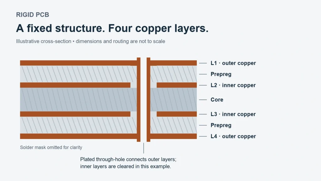
A plated through-hole can connect selected copper layers through its conductive barrel. As explained in Eurocircuits’ isolation guidance, clearance separates an unconnected hole from adjacent copper; passing through a layer does not itself establish a connection. This illustration shows construction, not a production stackup. Dielectric thicknesses, copper distribution and layer assignments still need agreement with the fabricator.
Choosing Materials, Thickness and Layer Count
Choose rigid PCB materials and dimensions from requirements, then confirm that the proposed combination can be fabricated and assembled.
| Exigence | Decision it influences | Confirmation needed |
|---|---|---|
| Enclosure, supports and connectors | Outline and finished thickness | Mechanical fit and connector specification |
| Routing density and signal return paths | Layer count and stackup | Placement, routing and electrical review |
| Current and heat dissipation | Copper, geometry and thermal paths | Temperature-rise assessment |
| Assembly and service environment | Laminate grade and construction | Process compatibility and environmental requirements |
FR4 is a family, not a complete material specification. For example, Isola’s FR408HR manufacturer page describes a multifunctional resin system reinforced with E-glass fabric. Naming the actual laminate helps distinguish properties that the broad FR4 label leaves unspecified.
Thermal properties need separate interpretations. Isola’s 370HR page reports a glass transition temperature (Tg) of 180 °C measured by differential scanning calorimetry (DSC), a decomposition temperature (Td) of 340 °C at 5% mass loss, and a relative thermal index (RTI) of 130°C referenced to UL 796. Tg concerns a change in material behavior; Td concerns decomposition under test conditions; RTI concerns long-term thermal aging under its evaluation conditions. None alone sets a finished board’s allowable operating temperature.
Consult the current manufacturer datasheet for test methods and applicability. Likewise, dielectric constant and dissipation factor need frequency and test context. The FR-4 material properties reference expands these distinctions. High-density interconnect (HDI) features address interconnection density; specify them separately from the board’s material and layer count.
Rigid vs Flexible PCB: When Does the Choice Change?
The choice changes when movement, packaging or interconnection requirements outweigh the advantages of a fixed board.
| Construction | Movement and packaging | Support and interconnection | Cost drivers |
|---|---|---|---|
| Rigide | Fixed shape in service | Stable component mounting; separate cables or connectors where needed | Area, layers, material, holes and assembly |
| Fléchissez. | Can accommodate installation bends or designed movement | Component regions may need reinforcement; can connect separated regions | Construction, reinforcement, bend requirements and assembly handling |
| Rigide-flexible | Integrates rigid regions with flexible sections | Supports components on rigid regions and connects them through flex | Integrated stackup, fabrication complexity and yield requirements |
A moving interconnect needs a construction designed for that movement. Making a rigid board thinner does not establish repeated-bend capability.
Compare total assembly cost alongside bare-board price. A flex or rigid-flex design may remove connectors or assembly operations, but those savings depend on the actual architecture and volumes. No construction has an unconditional reliability or thermal advantage. Use the flex PCB construction and comparison guide for the fuller comparison rather than transferring bend rules between technologies.
Applications That Favor a Fixed Board
Rigid boards suit applications where component support and stable mounting matter more than circuit movement.
A stationary industrial controller may need screw mounting, accessible terminal blocks and defined clearances inside an enclosure. Connector loads and vibration still require mechanical consideration.
A fixed communications board may benefit from internal reference planes and controlled routing geometry. Whether it needs a different laminate depends on its signal requirements, frequencies and loss budget, not the communications label alone.
Un LED or control assembly may need a firm mounting surface and a deliberate path for heat to reach a heatsink or enclosure. A rigid construction alone does not establish adequate heat removal.
These applications identify useful starting conditions. They do not determine laminate grade, layer count or suitability for a regulated product. Those decisions require project-specific evidence.
How Rigid PCB Manufacturing Works
Rigid PCB manufacturing turns patterned copper and insulating materials into a bare board. The following is a simplified multilayer overview; detailed operations and their order vary by process.
- Pattern the inner layers. Imaging and etching form circuitry on copper-clad cores before the layers are enclosed.
- Laminate the stack. Patterned cores, prepreg and outer copper foil are aligned and bonded.
- Drill and prepare hole walls. Drilling and conductive hole-wall treatment prepare connections for copper plating.
- Form the outer circuitry. Outer-layer imaging defines the pattern for plating and etching. In a pattern-plating process, copper and an etch-resistant metal are deposited before unwanted copper is etched away.
- Finish, profile and test. Solder mask, surface finish, markings, machining and agreed inspection/electrical testing complete the bare board. Their detailed order depends on the process.
Eurocircuits’ production inspection sequence distinguishes inner-layer processing, bonding, drilling, conductive hole treatment, outer imaging, plating and outer etching. The outer copper foil does not become finished circuitry during inner-layer etching.
Component assembly is a separate stage involving placement and soldering of surface-mount or through-hole parts. Bare-board electrical testing does not qualify the finished system’s function, safety or environmental durability. Those require their own validation plan.
Design Decisions to Confirm Before Fabrication
Confirm the construction and acceptance requirements before treating fabrication data as ready for release.
- Stackup and material: Agree on laminate, layer assignments and any substitution approval process.
- Thickness and fit: Check the finished board against connectors, enclosure features and mounting hardware.
- Copper and temperature rise: Assess current paths, copper geometry and heat removal under expected conditions.
- Holes and support: Resolve plated and non-plated holes, clearances and mechanical loads.
- Inspection and test: Specify the required acceptance criteria and test deliverables.
La official IPC document revision table identifies documents including IPC-2222, Sectional Design Standard for Rigid Organic Printed Boards, et IPC-A-600, Acceptability of Printed Boards. These titles identify relevant subjects; citing the table does not establish applicable clauses, product compliance or certification.
Cost depends on area, quantities, layer count, laminate, drill complexity, panel utilization, finishes and tolerances. A tighter requirement should serve a functional need because it can change available processes and price. Use the PCB design for manufacturing (DFM) checklist for the detailed release workflow rather than relying on universal trace, hole or thickness rules.
Worked Example: Selecting a Fixed Controller Board
A four-layer rigid PCB is a possible starting point for a fixed controller, but requirements and layout evidence must support the choice. This example is hypothetical, unvalidated and not a fabrication release instruction.
Start with the requirements
Assume a 24 V DC controller occupies an 80 × 60 mm mounting area in a fixed enclosure. Four screw supports carry the board, and stationary terminal blocks connect field wiring. The circuit includes a switching regulator and control signals; assembly uses surface-mount parts and soldered connectors. These dimensions and the supply value are invented example inputs, not measured results or recommended ratings.
Because all board connections remain stationary and the mounting area accepts a flat assembly, choose rigid construction for this example. A flexible circuit would need a separate packaging or movement requirement to justify its evaluation.
The actual current, ambient temperature, connector part numbers and assembly profile remain unspecified. “Low voltage” does not establish safe spacing, acceptable temperature rise or regulatory suitability.
Translate requirements into board decisions
| Exigence | Proposed choice | Reason | Approval still needed |
|---|---|---|---|
| Fixed enclosure and screw mounting | Rigid construction | Supports a fixed component layout | Outline, supports and load checks |
| Regulator and control-signal routing | Four copper layers | Candidate for routing with a ground reference | Layout and return-path review |
| No special material need yet established | Candidate FR4 laminate | Starting material family for evaluation | Exact grade and assembly compatibility |
| Connector interfaces | Thickness left open | Must match connector and enclosure | Connector data and mechanical fit |
| Conversion de puissance | Copper and heat paths left open | Dissipation depends on circuit and layout | Loss estimate and thermal validation |
A possible layer assignment is top components/signals, inner ground, inner assigned power/signals and bottom signals/components. It is a proposal, not evidence that four layers are necessary or sufficient. A successful two-layer layout might meet the requirements; denser routing might require another construction.
Show what would change the decision
Movement between enclosure sections could favor a flex interconnect. Higher temperatures or tighter electrical-loss requirements could change the laminate. Connector fit could change thickness, while thermal results could change copper geometry or heat-removal provisions.
Example decision record: Candidate construction is four-layer rigid FR4. The fixed enclosure and mounting concept are assumptions, not approved inputs. Open approvals include mechanical fit, exact laminate, stackup, routed layout, thermal behavior, assembly compatibility and fabricator acceptance. No production approval is implied.
Questions fréquemment posées
Is every rigid PCB made from FR4?
No. Rigid describes mechanical construction, while FR4 identifies a material family. Other laminate and substrate systems can provide rigid construction. Specify the actual material and required properties rather than assuming the word “rigid” establishes thermal or electrical performance.
Can a thin rigid board replace a flexible circuit?
Only if the application requirements support that substitution. A thin rigid board can deflect, but deflection does not establish suitability for installation bends or repeated movement. Evaluate the intended mechanical duty and interconnections before choosing the construction.
Are rigid boards always cheaper than flexible boards?
No. Compare equivalent requirements and the complete assembly. Bare-board complexity, material, quantity and panel utilization affect fabrication cost; connectors, cables, handling and assembly operations affect system cost. A price comparison needs a defined design and scope.
What files are needed for a rigid-board quote?
Provide fabrication data, drill data, a fabrication drawing, proposed stackup and material, quantities, and inspection or test requirements. Identify unresolved choices explicitly. Component assembly adds a bill of materials and placement information; confirm the supplier’s preferred formats and required supporting files.
Turn the Requirements into a Reviewable Specification
Begin with the enclosure, connectors, circuit and operating conditions, then propose a construction with unresolved inputs clearly identified. For a fabrication enquiry, provide that package through the rigid PCB manufacturing page. Request confirmation of material, stackup, fit and acceptance requirements before release.
Prepared for LEADHUI PCB. About the company · Contact LEADHUI PCB