Blog
Ici, vous pouvez acquérir des connaissances professionnelles couvrant toute la chaîne, de la conception PCB à l'assemblage, ainsi qu'une analyse précise des dernières tendances de l'industrie électronique.
Industrial PCB Production: Process & QA
Industrial PCB production turns an approved circuit-board design into bare boards and, when ordered, populated assemblies for industrial equipment. The route includes fabrication, component assembly, inspection and agreed testing. Approval depends on the specified build, operating conditions and acceptance criteria. A motor controller, sensor interface and cabinet-mounted control board can require different materials, mechanical support…
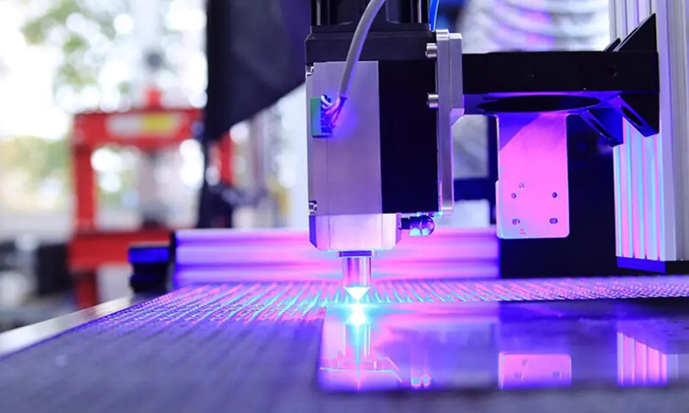
PCB en aluminium : conception thermique et matériaux
An aluminum PCB is a printed circuit board that combines copper circuitry, an electrically insulating thermal dielectric and an aluminum base. The dielectric carries heat toward the metal while separating the circuit electrically. This construction is useful for LED lighting and power electronics when the board, mounting interface and cooling surface form a suitable heat…
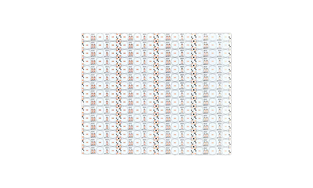
PCB HDI : empilage, microvias et conception
An HDI PCB, or high-density interconnect printed circuit board, uses fine conductors and compact interlayer connections to fit more wiring into a given area. Laser-drilled microvias and thin buildup layers help connect dense component pads without using a full-thickness hole at every connection. The design question is whether those features solve a routing constraint worth…

PCB rigide : matériaux, construction et choix de conception
A rigid PCB, or rigid printed circuit board, supports components and connects them through copper conductors on a substrate designed to retain its shape in service. It suits electronics whose circuitry stays fixed within an enclosure, rather than bending during use. Choosing one means matching its construction to the circuit, mounting, connectors and environment. Layer…

Circuit imprimé flexible : types, matériaux, empilage et règles de conception
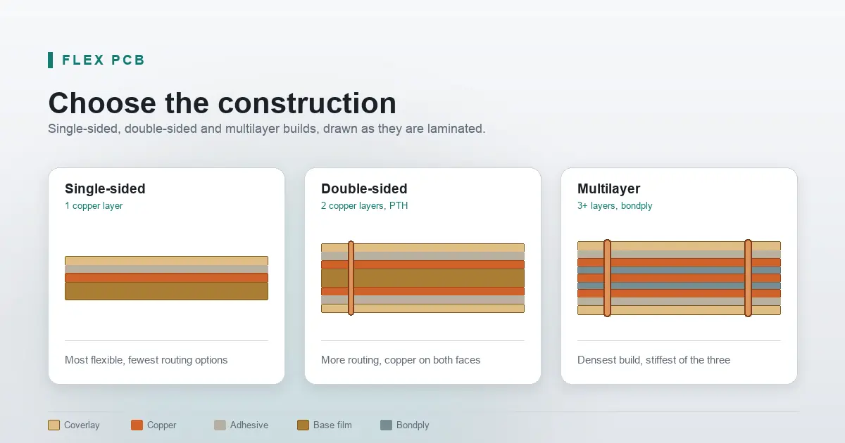
A flex PCB is a circuit built on a flexible polymer film, usually polyimide, with copper conductors bonded to it and a coverlay protecting them. That is the definition, and it is the part already answered above the search results. It is not the part that decides whether your build works. Four questions decide that,…
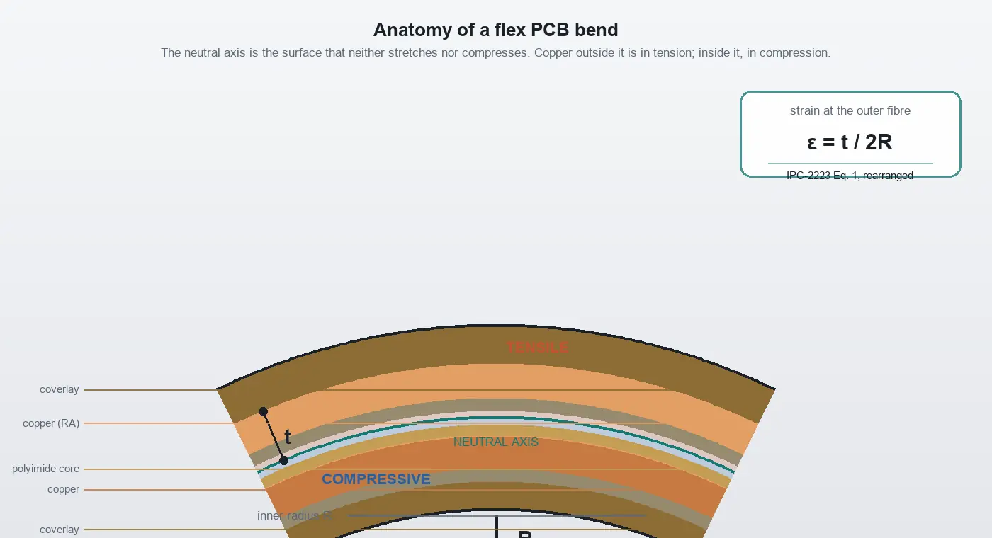
Rayon de courbure d’un circuit imprimé flexible : comment le calculer et le spécifier
You have a stackup, a housing envelope, and a mechanical engineer asking for a flex PCB bend radius. The answer is not a lookup table; it is a strain calculation, and the multipliers in the tables are what that calculation returns once you fix a stackup. Every published multiplier, whether it reads 6×, 10×, 12×,…
Guide du brasage par refusion : procédé, profil et défauts
Reflow soldering is the process that attaches surface-mount components to a printed circuit board by heating stencilled solder paste until it melts, wets the component terminations and forms the joint on cooling. It is the primary assembly method for almost every modern electronic product, and it is the step where the most expensive mistakes become…
Qu’est-ce que l’inspection de pâte de soudure (SPI)? Mesures, défauts et contrôle de qualité
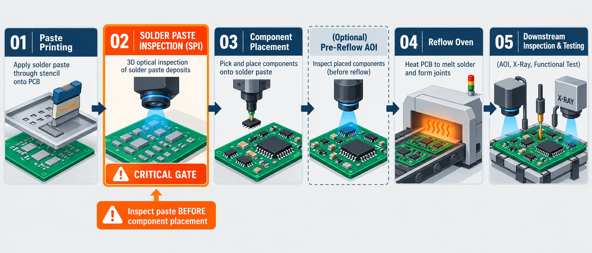
Solder paste inspection (SPI) checks paste deposited on a PCB after printing and before component placement. A 3D SPI system measures deposit volume, height, area, and alignment against programmed limits. It allows defective prints to be held and corrected before placement and reflow. For hardware engineers and PCBA buyers, the key decision is whether the…
Les 10 meilleurs logiciels de conception de circuits imprimés en 2026
KiCad is the strongest free desktop starting point for engineers choosing PCB design software in 2026. Altium Designer through Altium Develop is a strong paid choice for small teams that want shared libraries, browser review, and electrical–mechanical collaboration in one connected workflow. Both support serious board design; the purchasing decision is whether the surrounding workflow…
SMD Resistor Guide: Codes, Sizes, Footprints and Limits
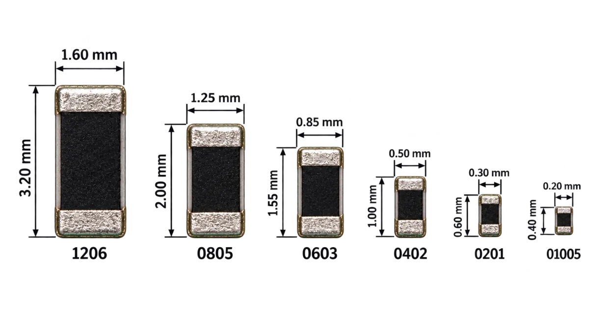
An SMD resistor is a fixed-value resistor in a leadless rectangular package that solders to pads on the surface of a printed circuit board rather than passing through holes. It is typically the most numerous component on a board, and the one most often specified from habit rather than from the datasheet. Most guides to…
Stratifié cuivré (CCL) : types, fabrication, performances et normes
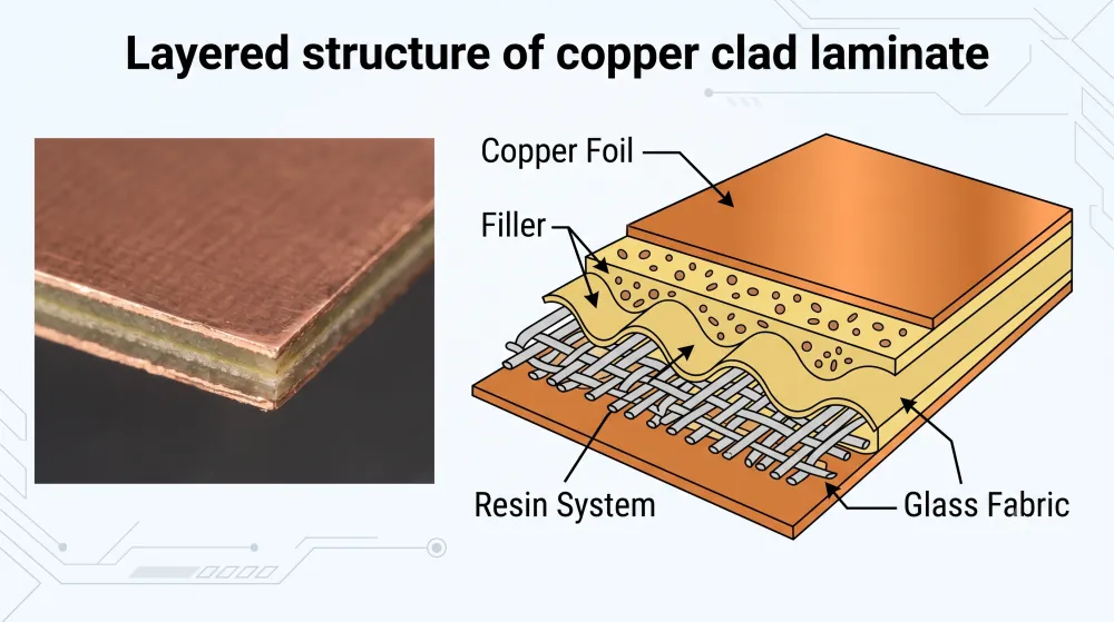
Copper clad laminate, or CCL, is a base material from which PCB conductors are formed. It consists of copper foil bonded to an insulating material such as cured glass-reinforced epoxy, a flexible polymer film, or a thermally conductive dielectric on a metal base. In a conventional multilayer rigid PCB, patterned CCL commonly becomes a core.…
JLCPCB vs PCBWay : quel fabricant de PCB convient à votre projet ? (2026)
For a straightforward PCB prototype or a small assembly order that fits JLCPCB’s Economic PCBA rules, start with JLCPCB, especially when the components are already in its inventory. For rigid-flex or extensive custom fabrication requirements, shortlist PCBWay early. These recommendations follow from JLCPCB’s economical assembly tier and PCBWay’s documented advanced manufacturing options. The JLCPCB vs…

What Is GND? Meaning, Types, and PCB Grounding Explained
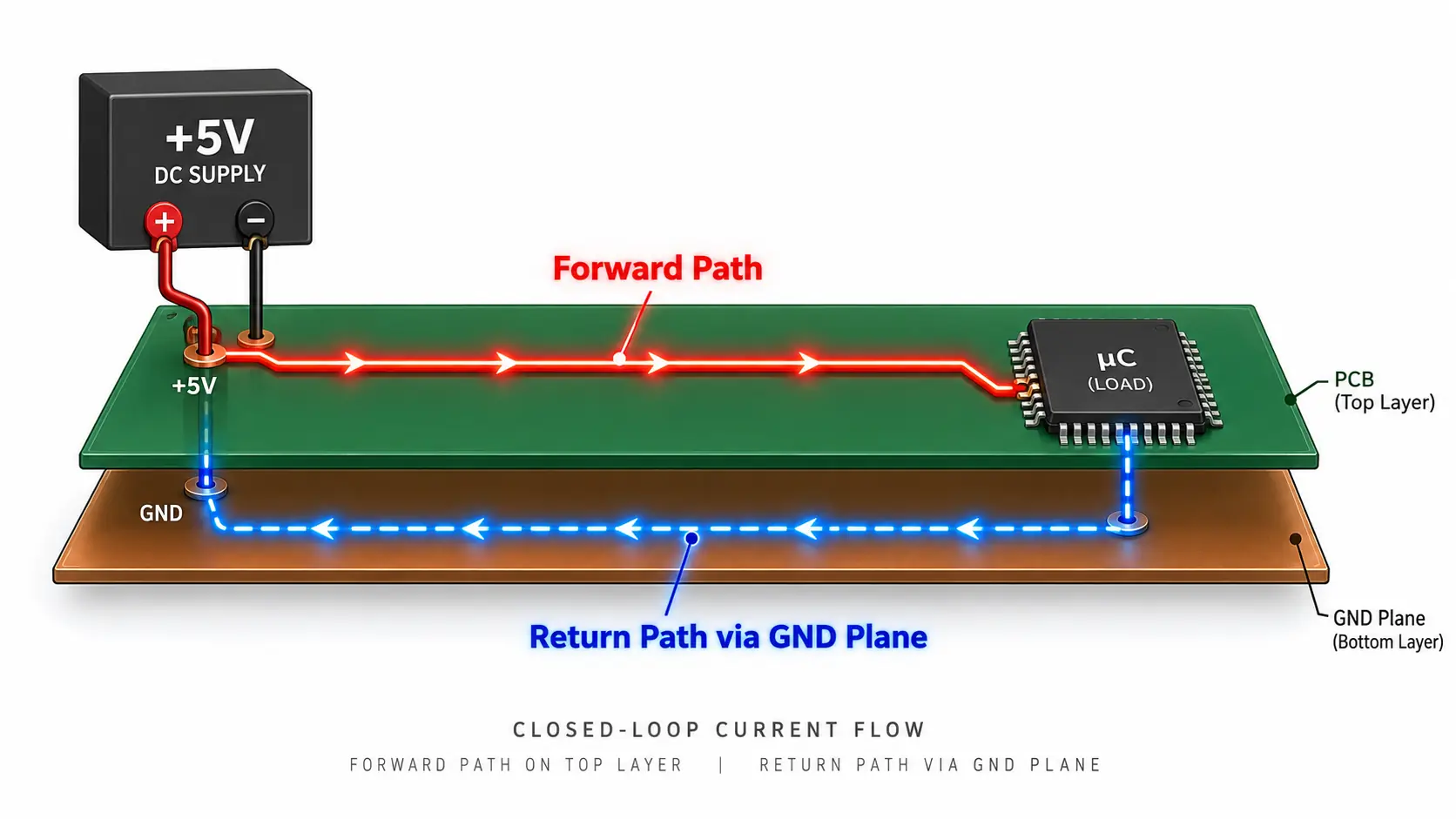
GND appears on almost every circuit diagram, PCB, power supply, and electronic module. It is often described as “zero volts” or “the negative terminal,” but neither description is universally correct. In electronics, GND stands for ground. It is the reference node against which other voltages are measured and, in many circuits, part of the path…
What Is a Through Hole? PCB Types, Uses, and Design Guide
A through hole is an opening that passes completely from one side of a printed circuit board (PCB) to the other. It may be plated with conductive copper to create an electrical connection, or left unplated for mechanical use. Through holes are commonly used for component leads, connectors, vias, mounting hardware, alignment pins, and slots.…

Que sont les boîtiers QFN ? Un guide pratique pour la conception et l'assemblage de PCB
Les boîtiers QFN apparaissent dans tout, des alimentations électriques et modules sans fil aux capteurs, microcontrôleurs et électronique automobile. Leur petite empreinte, leurs chemins électriques courts et leur transfert de chaleur efficace en font une alternative attrayante aux boîtiers à broches plus grands. Cependant, les mêmes connexions sous la face qui économisent de l’espace rendent également la conception de l’empreinte QFN, le soudage et l’inspection moins tolérants. Ainsi,…

Guide des matériaux PCB : types, propriétés et sélection
Le matériau du PCB affecte bien plus que la résistance physique d’une carte de circuit imprimé. Il influence l’impédance, la perte de signal, la dissipation thermique, la stabilité dimensionnelle, la fiabilité d’assemblage, la fabricabilité, le délai de livraison et le coût. Un matériau qui fonctionne bien pour un contrôleur de base peut échouer dans un module radar à 77 GHz, une carte LED à courant élevé ou un dispositif médical rigide-flexible.…

Conception de circuits imprimés d'impédance contrôlée : StackUp, spécifications et tests
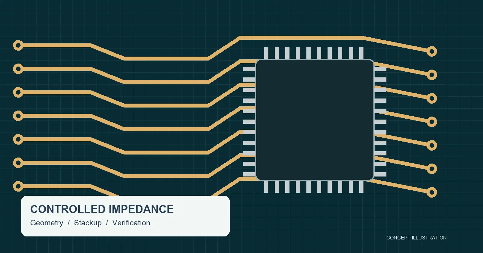
Controlled impedance is the practice of designing and manufacturing PCB traces so their characteristic impedance meets a specified target and tolerance. The result depends on the conductor geometry, dielectric construction, and reference planes. A complete requirement also states how the manufacturer will verify the finished structure. A note that says only “50 ohms” leaves important…
Résistance 10k : Code couleur, utilisations et comment choisir la bonne
Une résistance de 10k est un composant électrique passif avec une résistance nominale de 10 000 ohms (10kΩ). Dans la conception de circuits moderne, c'est l'une des valeurs les plus omniprésentes trouvées sur les plaques d'essai et les PCB de production. Les ingénieurs et les amateurs se tournent vers les résistances de 10k car elles atteignent un juste milieu électrique idéal : elles limitent le courant à des niveaux sûrs,…

Conception d’antenne PCB : implantation, matériaux et fabrication
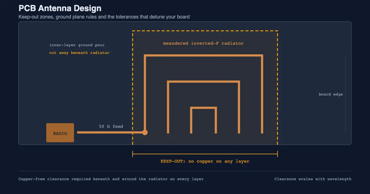
A PCB antenna is a copper trace or pattern etched directly onto a printed circuit board that transmits and receives radio frequency electromagnetic waves. It is the cheapest way to give a product wireless connectivity, because it adds no connector, no cable and no bill-of-materials line. It is also the part of a design most…
LED Anode et Cathode : Comment identifier les bornes positive et négative
Une LED (diode électroluminescente) est un dispositif semi-conducteur polarisé qui permet au courant de circuler dans une seule direction. Pour allumer une LED, vous devez connecter correctement ses bornes positive et négative dans votre circuit. Sur les LED traversantes standard, la patte la plus longue et le côté arrondi représentent l'anode, tandis que la patte la plus courte et le…