A multilayer PCB contains three or more conductive copper layers separated by insulating dielectric and bonded into one board. The count refers to copper layers, not prepreg, core sheets or solder mask. It does not, by itself, tell you whether the board is rigid or flexible, how thick it is or how well it will perform.
Choosing a construction means comparing the signals, their return paths, routing space and fabrication constraints. The fictional measurement board below carries the same requirements through two-, four- and six-layer options so the outstanding decisions are visible. For the mechanical and material choices behind a rigid board, see the rigid PCB construction guide.
Principais conclusões
- Layer count, mechanical construction and finished thickness are separate specifications.
- A two-layer board can be viable when the design meets its requirements; four and six layers offer other ways to assign copper and routing.
- Check return paths, reference-plane continuity and layer transitions against the actual geometry and power distribution network.
- Cost depends on the complete build. Additional copper layers do not automatically require another lamination cycle.
- The example is fictional; all candidates and the required human engineering review remain pending.
What Is a Multilayer PCB?
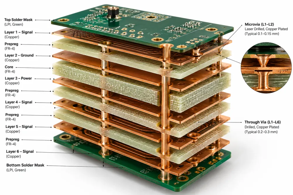
A single-sided PCB has one copper layer; a double-sided PCB has two. A multilayer circuit board has three or more copper layers. Even counts are common, but odd counts are possible. The layers may carry signals, power or ground, depending on the design.
Layer count describes electrical construction, while rigid, flex and rigid-flex describe mechanical construction. A multilayer board can use any of those mechanical forms. Its finished thickness depends on the actual copper and dielectric construction, so a layer count alone does not specify it.
O flex PCB construction guide covers flexible materials and mechanical design.
2-Layer vs 4-Layer vs 6-Layer PCB: What Changes?
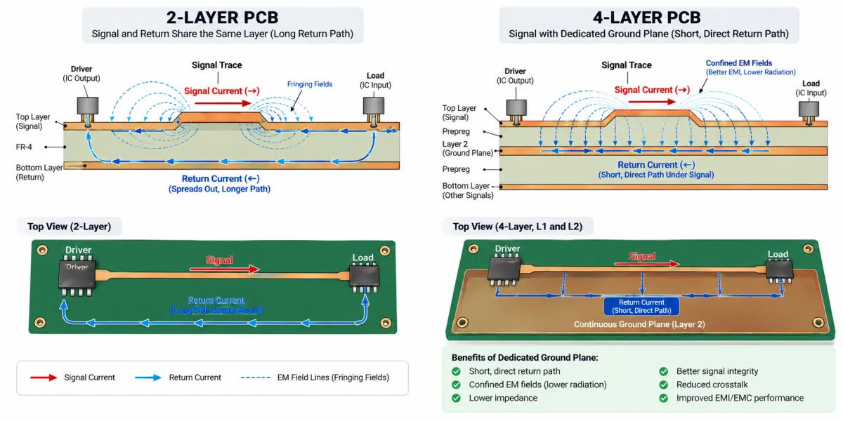
The examples below compare possible layer assignments, not standard recipes. A reference plane is a copper region that provides a path for signal return current; its usefulness depends on the geometry and continuity of that region. On a small screen, scroll the table sideways to see all columns.
Layer-count comparison
| Candidata | Example copper roles | Routing and reference considerations | Fabrication consideration | When to evaluate |
|---|---|---|---|---|
| 2 layers | Signal and ground copper on both sides as needed | Routing can interrupt available ground copper. Check each critical return path. | No internal copper layers; actual complexity still depends on the features and tolerances. | When placement, routing and electrical requirements may fit on two sides. |
| 4 layers | Signal / ground / power / signal | Two outer signal layers, with inner copper available for references and power. Check the power-plane reference and transitions. | Inner layers need alignment; material and thickness choices remain open. | When internal ground and power regions merit comparison with a two-layer layout. |
| 6 layers | Signal / ground / signal / power / ground / signal | An additional proposed signal layer creates routing choices. Its return can involve both adjacent planes. | More internal copper requires a suitable construction and alignment plan. | When routing or reference needs suggest evaluating another signal layer. |
More layers do not guarantee lower emissions, controlled impedance or a smaller board. A two-layer design can work if its actual routing, electrical behavior and other requirements are acceptable. All three candidates need layout and fabrication review.
How a Multilayer Circuit Board Is Built
A multilayer board combines patterned copper with insulating materials, then uses plated connections where the design calls for layers to connect.
Copper, core and prepreg
Copper forms traces, pads and planes. A núcleo is a cured laminate, often supplied with copper on its faces. Pré-impregnado is reinforcement impregnated with partially cured resin; it bonds layers during lamination. The number and arrangement of cores, prepregs and copper foils depend on the selected construction. A stackup drawing records their order and the specifications needed to build the board.
How vias connect selected layers
A plated through-hole spans the board. A blind via connects an outer layer to an internal layer, while a buried via connects internal layers without reaching either surface. Siemens’ 2025 explanation of blind and buried vias describes these structures and the manufacturing tradeoffs they can introduce.
A plated barrel passing through an internal layer does not automatically connect to its copper. Pads and clearances determine which layers it joins. Choose via spans with the fabricator’s process and design rules in mind; the guia de vias de PCB covers the options, and the HDI PCB guide addresses buildup and microvia structures.
Reading a 4-Layer PCB Stackup and a 6-Layer Stackup
Read a stackup from one board surface to the other, assigning a purpose to every copper layer. These two examples show proposed roles, not finished fabrication stackups. Plane shapes, dielectric geometry and connections still need design work.
Four-layer PCB stackup
One candidate is L1 signal / L2 ground / L3 power / L4 signal. Where L2 ground is continuous and the geometry supports it, it can provide a nearby reference for L1 signals. L4 signals lie next to L3 power; their return paths depend on the power copper’s continuity, geometry and power distribution network. Altera’s power and ground layer guidance describes using either power or ground as a reference and explains why discontinuities in power copper need attention.
A signal changing layers may also change references. Evaluate how its return current transfers between the relevant reference regions, including the power network and the placement and impedance of decoupling. Eric Bogatin’s discussion of reference-plane transitions explains why the plane connection and capacitor impedance matter. A capacitor’s presence alone does not prove that the transition is acceptable. Power-plane gaps or islands also need attention.
Analog Devices’ 2022 mixed-signal layout guidance discusses a four-layer example and return-path considerations for high-performance data acquisition. It is useful context, not a universal minimum layer count.
Six-layer PCB stackup
Another candidate is L1 signal / L2 ground / L3 signal / L4 power / L5 ground / L6 signal. L1 and L6 are adjacent to ground layers, which can serve as references where the actual copper and geometry support them. L3 is bounded by L2 ground and L4 power: its fields and return currents can involve both planes, depending on their geometry and the power distribution network.
Review the paths for each signal and each transition, rather than assuming layer labels establish continuity. Ask the fabricator about stackup symmetry and copper distribution as mechanical and manufacturing checks; symmetry alone does not guarantee flatness. If impedance control is required, the controlled impedance PCB guide covers specifications and verification.
Worked Example: Choosing Layers for a Compact Measurement Board
This teaching example compares the same fictional requirements across all three candidates. No customer board, measured result or completed design review is implied.
State the requirements and assumptions
Suppose a rigid mixed-signal board must fit a 55 × 40 mm outline, sample a 0–2 V sensor signal up to 100 Hz with a 16-bit analog-to-digital converter, and communicate over a serial peripheral interface (SPI) link with a 1 MHz clock. For this exercise, allocate the board at most 1 mV root-mean-square (RMS) noise referred to the converter input within a nominal 0–100 Hz measurement band. Assume the sensor connector and converter can be placed on the same side, with the SPI connector toward the opposite board edge. The provisional finished thickness is 1,6 mm, subject to enclosure and connector fit. These values are invented design targets, not measurements or requirements for a particular product.
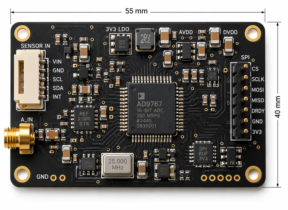
If the converter’s full-scale range is 2 V, one ideal 16-bit code step is approximately 2 V / 65,536, or 30.5 microvolts at the converter input. In that case, the allocated 1 mV RMS, referred to the same input, is approximately 33 code steps RMS. A code step is a voltage interval, while RMS noise describes noise magnitude over the stated band. The noise allocation must be judged against the actual measurement resolution and accuracy needs; this comparison alone does not establish effective resolution or a measurement result. The sensor’s 0–2 V signal range does not by itself establish the converter’s full-scale range.
Actual component selection, sensor impedance, supply noise, edge rise and fall times, component locations, signal routes and lengths, plane shapes, routing density, temperature, available fabrication stackups, connector tolerances and test requirements are unknown. Specify the measurement setup, bandwidth and operating conditions before testing the noise target. Converter resolution alone does not establish measurement accuracy, and the SPI clock rate alone does not establish the edge speed or whether impedance control is needed.
Compare the candidates
Each row applies the same outline, sensor signal, noise target, interface and provisional thickness above. Copper roles and return paths are proposals to investigate, not claims that the board will route or pass a test. On a small screen, scroll the table sideways to see all columns.
Worked example comparison
| Candidate and proposed copper roles | Possible return path | Routing and open checks | Possible manufacturing tradeoff | Approval |
|---|---|---|---|---|
| 2 layers: L1 signals and ground fill; L2 ground where possible, with signals as needed | Return paths depend on the complete circuit and frequency-dependent impedances; traces and holes can interrupt ground copper[cite: 2]. | Test whether sensor and SPI routes fit while preserving a suitable ground path; define and verify the 1 mV RMS noise target[cite: 2]. | No inner copper; fine features or tight tolerances may still affect the build and quote[cite: 2]. | Pending[cite: 2] |
| 4 layers: L1 signal / L2 ground / L3 power / L4 signal | L1 may reference L2. L4 may reference L3; transitions need a suitable path through the power distribution network[cite: 2]. | Check whether sensor routing can use L1 over continuous L2, whether SPI fits and whether noise, L4 returns and thickness meet requirements[cite: 2]. | Inner-layer registration and a construction meeting the 1.6 mm target need review[cite: 2]. | Pending[cite: 2] |
| 6 layers: L1 signal / L2 ground / L3 signal / L4 power / L5 ground / L6 signal | L1 and L6 are next to ground; L3 lies between ground and power and its return can involve both[cite: 2]. | Check whether SPI or other routes need the extra layer, then assess L3, transitions, thickness and the same noise target[cite: 2]. | More internal copper and alignment requirements may affect construction and cost; confirm the available process[cite: 2]. | Pending[cite: 2] |
Carry the four-layer candidate forward provisionally because the sensor and converter could be placed on L1 over an L2 ground region, while other routes use the remaining space. The separate power layer is another feature to evaluate. This is a layout hypothesis, not evidence that the noise target or any other requirement passes. Two layers remain viable if a real layout meets the same electrical and mechanical requirements. Review six layers if routing or reference needs justify another signal layer and a suitable construction is available.
Record the review decision
Use a short decision record to keep assumptions from becoming an accidental approval:
- Requirement: The fictional outline, sensor signal, noise objective, converter, SPI clock and provisional thickness above apply to every candidate. Other performance limits and a test method remain to be defined.
- Candidate and rationale: Four layers are provisionally carried forward for evaluation of ground, power and routing. Two and six layers remain alternatives.
- Status and reviewer roles: Design review and approval are pending for all three candidates. Intended review roles include the board designer, electrical or signal-integrity reviewer, mechanical engineer and fabricator; no reviewer has been appointed in this example.
- Missing verification: Obtain device requirements and edge times, a real placement and routed geometry, return-path and power-network analysis, an available stackup, thickness and connector tolerances, and agreed tests. Revise a candidate if its routing interrupts a needed return path or fails a requirement.
- Noise-test plan: Before comparing candidates, agree the sensor input condition or representative source impedance, operating conditions, sampling and filtering. Define the practical lower frequency limit or observation time, treatment of slow drift, and effective measurement bandwidth consistent with the nominal band. Specify which noise sources are included in the board allocation, including how sensor and test-equipment noise will be handled. Define how to calculate RMS noise referred to the converter input over that band. Against the example’s allocated limit, a result at or below 1 mV RMS is a pass for that noise criterion only; no result exists yet.
- Approval condition: Responsible engineers must check the chosen design against actual requirements, and the intended fabricator must confirm the proposed construction before the design can be released.
A qualified human engineer must separately review this educational example, its layer roles and the diagrams before publication. That review is pending and would not approve a board for manufacture.
Multilayer PCB Manufacturing: From Inner Layers to Test
A conventional rigid multilayer fabrication sequence forms the internal circuits, bonds the stack and then creates the outer circuits and connections. The order and inspection points vary with the design and supplier. Flex and rigid-flex constructions can use flexible bondply and coverlay, with a process specific to their materials and design.
- Prepare inner layers. Image and etch the required inner copper patterns, then inspect them before they become enclosed.
- Align and laminate. Arrange cores, prepreg and outer copper, register the layers, and bond the stack under heat and pressure.
- Drill and metallize. Make the specified holes and plate the applicable barrels to provide designed connections.
- Form the outer circuits. Image, plate and etch the outer copper as required by the process, then apply solder mask and the specified surface finish.
- Profile, inspect and test. Form the board outline and perform the inspections and electrical tests agreed for the order.
Eurocircuits’ registration guidance explains why the alignment of layers and drilled features matters. Its production inspection sequence illustrates checkpoints in one manufacturer’s process; it does not establish another supplier’s tolerances or test scope.
Algumas vias cegas ou enterradas exigem processamento em etapas e laminação sequencial. Várias camadas de cobre também podem ser combinadas em um único ciclo de laminação, portanto, adicionar camadas nem sempre implica outro ciclo. Um teste acordado de circuito aberto/curto-circuito verifica a conectividade e o isolamento dentro do escopo definido; ele não comprova a integridade completa do sinal, o desempenho térmico ou a qualificação do produto. A montagem acrescenta componentes e constitui um escopo separado; o guia de produção industrial de PCBs descreve esse fluxo de trabalho mais amplo.
Verificações de projeto de PCB multicamada antes da liberação
Revise o layout real e o empilhamento de camadas proposto em conjunto antes de liberar os arquivos de fabricação:
- Referências e transições: Verifique a continuidade do cobre próximo a sinais críticos, lacunas, mudanças de camada e caminhos relevantes da rede de alimentação. Analise, na geometria real, os cruzamentos de cortes nos planos.
- Materiais e geometria: Confirme o laminado, o espaçamento dielétrico, os requisitos de cobre e a espessura final com o fabricante. Se for necessária impedância controlada, especifique as redes, os valores-alvo e as tolerâncias, e combine como isso será verificado.
- Cobre e registro: Revise a simetria das camadas, a distribuição de cobre, os pads, as folgas e as tolerâncias de alinhamento para o processo proposto.
- Vias e furos: Verifique os tipos, tamanhos e extensões dos furos, bem como as conexões pretendidas, de acordo com o empilhamento de camadas e as regras do fornecedor.
- Encaixe mecânico: Verifique o contorno, a tolerância de espessura, a montagem e os conectores em relação ao invólucro e aos requisitos de montagem.
- Aceitação: Combine o escopo da inspeção e dos testes elétricos, além de quaisquer verificações térmicas, ambientais ou funcionais necessárias para o produto.
Uma lista de verificação preenchida deve apontar para evidências do layout real e do fornecedor, e não apenas para os nomes das camadas. Registre os itens pendentes e seus responsáveis antes da liberação.
O que determina o custo de uma PCB multicamada?
O custo de uma PCB multicamada depende da construção completa e do pedido, não apenas da quantidade de camadas de cobre.
Fatores de custo
| Fator | Possível consequência a discutir no orçamento |
|---|---|
| Quantidade de camadas e área da placa | Camadas internas adicionais podem exigir mais material, geração de imagens e inspeção. Placas maiores podem reduzir a quantidade que cabe em um painel de fabricação. |
| Laminado e espessura | Um laminado especializado ou uma tolerância rigorosa de espessura final pode limitar as opções de materiais e de empilhamento de camadas, afetando o custo dos materiais ou do processamento. |
| Tipo e extensão das vias | Vias cegas ou enterradas podem exigir furação adicional ou processamento em etapas, dependendo de suas extensões e da construção escolhida. |
| Tolerâncias de características e registro | Trilhas mais finas, folgas menores ou alinhamento mais rigoroso entre camadas podem exigir processamento ou inspeção mais rigorosos, dependendo do processo do fornecedor. |
| Acabamento, inspeção e teste | Alguns acabamentos exigem materiais ou processamento diferentes; inspeções ou testes adicionais podem acrescentar trabalho ao escopo de aceitação acordado. |
| Quantidade e prazo solicitado | Quantidades maiores podem diluir o trabalho de preparação em mais placas, enquanto o aproveitamento do painel e as restrições de prazo podem afetar o orçamento. |
Compare os orçamentos usando os mesmos requisitos funcionais, quantidade, acabamento, tolerâncias, testes e prazo solicitado. Inclua a montagem separadamente, quando necessário. Uma abordagem com maior densidade de vias ou uma camada adicional pode alterar o custo de fabricação, mas a compensação geral depende de cada projeto.
O que enviar para uma análise de fabricação
Envie uma revisão controlada dos arquivos e informações suficientes para que o fabricante entenda o que está definido e o que ainda está em aberto:
- Desenhos das camadas de cobre e sua identificação, dados de furação, contorno da placa e ranhuras.
- Ordem proposta das camadas, materiais, espessura final e tolerâncias, além dos requisitos de cobre.
- Tipos e extensões das vias, folgas relevantes e quaisquer requisitos de impedância controlada.
- Quantidade, máscara de solda e acabamento, requisitos de inspeção e teste elétrico e prazo de entrega solicitado.
- Opções em aberto, substituições permitidas e a pessoa ou função autorizada a aprovar alterações.
Visão geral do formato Gerber da Ucamco descreve como o formato transmite dados de imagem de PCB e atributos. Por si só, ele não define um pacote completo de liberação. Confirme os formatos aceitos pelo fabricante escolhido e a documentação complementar. A montagem também exige uma lista de materiais e dados de posicionamento adequados; o guia de Gerber, BOM, CPL e empilhamento de camadas explica esses arquivos de transferência.
Perguntas frequentes
O que é uma PCB de quatro camadas?
Uma PCB de quatro camadas tem quatro camadas condutoras de cobre separadas por material dielétrico. Uma configuração comum, apresentada apenas como exemplo, usa duas camadas externas para sinais e duas internas para terra e alimentação, mas as funções e os materiais reais dependem do projeto.
Quanto custa uma PCB de quatro camadas?
Uma cotação precisa exige a definição da placa e da quantidade. Dimensões, materiais, cobre, furos, tolerâncias, acabamento, testes e prazo solicitado são fatores importantes. Ao comparar alternativas, solicite uma cotação com os mesmos requisitos.
Toda PCB multicamada precisa de vias cegas ou enterradas?
Não. Uma PCB multicamada pode usar vias passantes metalizadas para conectar camadas específicas. Vias cegas ou enterradas são alternativas quando o roteamento e a construção exigem; confirme com o fabricante as camadas abrangidas e o processo necessário.
Adicionar camadas melhora automaticamente a integridade do sinal?
Não. Camadas adicionais oferecem mais opções, mas o resultado depende da continuidade dos planos, da geometria das trilhas, dos caminhos de retorno, das transições e da distribuição de energia. Avalie o layout real e verifique os requisitos aplicáveis aos sinais.
Solicite uma análise de fabricação
Para uma consulta específica do projeto, acesse Fabricação de PCBs e informe o contorno, a estrutura de camadas proposta, os requisitos de cobre e vias, a quantidade e a inspeção solicitada. Identifique as escolhas ainda não definidas e pergunte se a construção pretendida pode ser atendida antes de aprovar substituições ou fazer um pedido.