The standard PCB thickness for many general-purpose rigid boards is 1.6 mm nominal finished thickness, approximately 0.063 inch or 63 mil. JLCPCB’s standard PCB thickness guide, updated September 9, 2026, describes 1.6 mm as a common standard thickness. Other dimensions are used too, as described in Altium’s board thickness and stackup guide. A nominal value is a target, not a measurement or an acceptance range. Before selecting one, check the finished board’s tolerance against the actual connector, enclosure and stackup requirements.
Principais conclusões
- A 1.6 mm nominal thickness is a common starting point for rigid PCBs. The design and fabrication agreement determine the dimension for a particular board.
- Nominal thickness and tolerance define a range. Connector fit needs that range checked at the same measurement surfaces used in the connector drawing.
- Total board thickness, copper thickness and the dielectric spacing between selected layers are different dimensions.
- Document the measurement location, finished surfaces, tolerance and inspection method, then obtain fabrication and engineering approval before release.
What Is the Standard PCB Thickness?
A common standard circuit board thickness is 1.6 mm nominal, but that is a convention rather than a mandatory size for every design. The controlled drawing and the agreed fabrication requirements define the target and acceptable limits for a specific board.
Metric and imperial labels that look similar are not identical:
- 1.60 mm = 0.06299 inch, approximately 63 mil.
- 0.062 inch = 1.5748 mm, approximately 1.57 mm.
- 1/16 inch = 1.5875 mm.
These values may be rounded together in conversation. On a drawing, keep the intended nominal dimension, units and tolerance explicit. The difference can matter when a connector or housing has a restricted clearance.
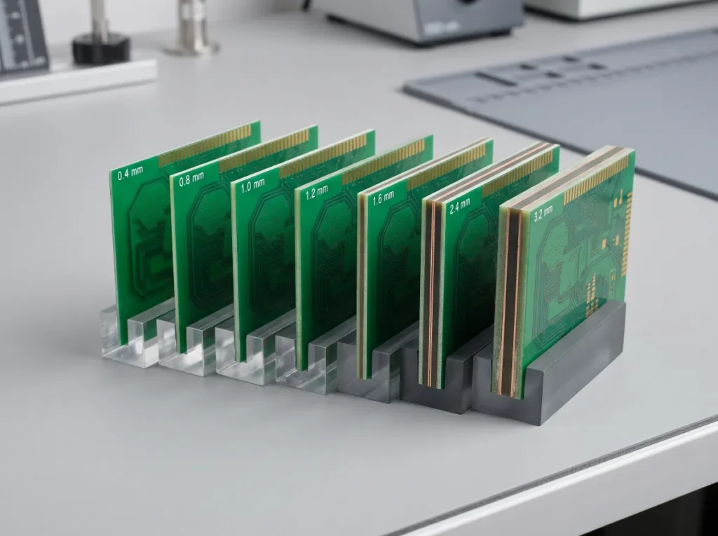
PCB Thickness Chart: Common Sizes in mm and Mils
The following nominal board thickness options appear on the PCB manufacturing capabilities page, checked October 29, 2026. The inch and mil values are rounded; one mil is 0.001 inch.
| Espessura nominal | Approx. inches | Approx. mils | When to consider it |
|---|---|---|---|
| 0,4 mm | 0.0157 | 15.75 | Low-profile layouts; review handling. |
| 0,6 mm | 0.0236 | 23.62 | Thin rigid builds; confirm support. |
| 0,8 mm | 0.0315 | 31.50 | Shallow housings; check deflection. |
| 1,0 mm | 0.0394 | 39.37 | Limited clearance; confirm the stackup. |
| 1,2 mm | 0.0472 | 47.24 | Where the mechanical interface calls for it. |
| 1,6 mm | 0.0630 | 62.99 | A common starting point; confirm fit. |
| 2,0 mm | 0.0787 | 78.74 | Where more stiffness is needed; check drilling. |
| 2.4 mm | 0.0945 | 94.49 | Thicker builds; review slots and via depth. |
| 3.2 mm | 0.1260 | 125.98 | Thicker builds; review drilling and fabrication. |
These are nominal values, not acceptance ranges. A listed size does not establish availability for every material, copper weight or layer count. Confirm the current options and the proposed construction with the fabricator.
What Does Finished PCB Thickness Include?
Finished PCB thickness describes a dimension across the completed board, but the surfaces and measurement location must be defined. A connector may control a different local dimension from the general board thickness on a fabrication drawing.
Board thickness, copper thickness and dielectric spacing
| Dimension | O que descreve | Por que isso importa |
|---|---|---|
| Finished board thickness | The complete board between specified surfaces | Connector and enclosure fit |
| Espessura do cobre | A specified conductive layer | Conductor geometry and fabrication |
| Dielectric spacing | Insulation between particular copper layers | Stackup and impedance calculations |
Copper weight is a separate specification from total board thickness. PCB Prime’s copper conversion reference puts 1 oz of copper per square foot at approximately 35 µm, or 0.035 mm, nominal thickness. Plating can add copper to outer layers, so finished copper can differ from the starting foil.
Where and how is thickness measured?
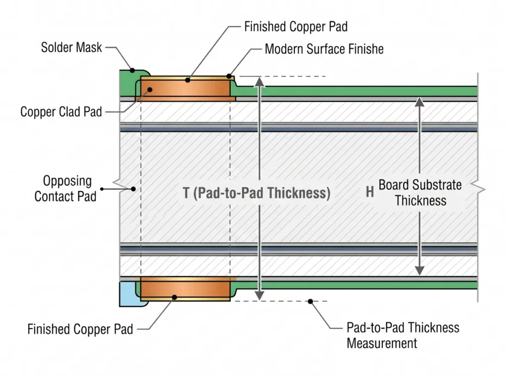
A rigid board’s construction can include cores, prepreg and copper layers. Plating, solder mask and surface finish can also affect a local measurement. Ask which surfaces the fabricator uses for its finished-thickness specification, whether mask and finish are included, and where and how it measures the board.
At a card edge, pad-to-pad thickness is the local distance between the specified finished connector pad surfaces on opposite sides of the board. A reading over solder mask elsewhere does not automatically describe that dimension.
How to Choose PCB Thickness for Your Design
Choose a nominal thickness only after checking the mechanical and fabrication constraints together. Use the actual product drawings and ask the fabricator to review the proposed construction.
| Requisito | Design question | Confirmação necessária |
|---|---|---|
| Connector or board slot | What card thickness range and surfaces does the drawing specify? | Compare both finished limits at the stated location. |
| Enclosure and mounting | Does the board clear the housing, standoffs and fasteners? | Check the allowed range and assembly clearances. |
| Support and handling | Can the board span its supports and withstand assembly loads? | Review deflection and the handling process. |
| Layer stack | Can the selected layers and dielectric spacings meet the target? | Approve the stackup and any impedance requirements. |
| Vias and drilling | Does board thickness change the hole depth-to-diameter ratio? | Confirm drill and plating feasibility. |
| Materials and supply | Are the materials and construction available at the target thickness? | Confirm options, cost and lead time for the build. |
For otherwise comparable boards, increasing thickness generally increases stiffness. Board dimensions, support span, material, layup and loads also affect deflection. A thin rigid board is not automatically a flex circuit; it should not be treated as one simply because it bends.
Layer count does not uniquely determine finished thickness. A different total thickness may require a stackup revision, but it does not by itself determine an impedance change. Impedance depends on the relevant trace geometry, dielectric spacing and materials. Review the proposed construction with the fabricator and use the guia de projeto de PCB com impedância controlada for the electrical specification. For material selection, see FR-4 PCB materials and design.
Worked Example: Will a 1.6 mm Board Fit a Card-Edge Connector?
A PCB thickness tolerance must be compared with the connector’s full permitted card range at the same surfaces. The following educational example combines a real connector drawing with a separate supplier’s published board tolerance. It is not a measured customer design or a qualification result.
Read the connector drawing
O Samtec HTEC8 drawing, revision N, retrieved October 29, 2026, gives the -01 card-thickness option a 1.57 mm nominal mating card with a ±0.157 mm pad-to-pad tolerance. Its calculated limits are:
1.57 – 0.157 = 1.413 mm minimum; 1.57 + 0.157 = 1.727 mm maximum.
The series drawing also includes a different card-thickness option. Check the exact connector part, current drawing revision, lead-in and all other mating requirements before using these numbers.
Compare the full board range
As a separate supplier example, JLCPCB’s capabilities page, checked October 29, 2026, lists a ±10% thickness tolerance for boards at least 1.0 mm thick. Applying that illustrative tolerance to a 1.60 mm nominal board gives:
1.60 × 0.90 = 1.44 mm minimum; 1.60 × 1.10 = 1.76 mm maximum.
If that board tolerance applied to the same pad-to-pad surfaces at the mating edge, its 1.76 mm upper limit would exceed the connector’s 1.727 mm upper limit by 0.033 mm. Its 1.44 mm lower limit would be 0.027 mm above the connector’s minimum. Under that condition, the board tolerance alone would not ensure that the entire permitted board range meets the connector’s thickness range.
The supplier page does not establish that its thickness tolerance uses those pad-to-pad surfaces. Obtain the measurement definition before comparing the physical requirements. Neither the published values nor this calculation proves that a particular manufactured card passes or fails.
Record a possible specification and open questions
One hypothetical request is 1.57 mm ±0.10 mm pad-to-pad at the mating edge, giving a range of 1.47 to 1.67 mm. On the same defined surfaces, that requested range sits inside the connector’s stated range by 0.057 mm at each limit.
| Requisito | Example range | Status |
|---|---|---|
| HTEC8 -01 mating card | 1.413 to 1.727 mm pad-to-pad | Published connector drawing; verify revision and other requirements. |
| Illustrative 1.60 mm board at ±10% | 1.44 to 1.76 mm | Published tolerance example; pad-to-pad equivalence unconfirmed. |
| Proposed 1.57 mm board at ±0.10 mm | 1.47 to 1.67 mm pad-to-pad | Hypothetical request; fabrication and inspection approval pending. |
The proposed tolerance is not a published fabricator capability. Confirm it can be produced and inspected, agree how finish and measurement uncertainty are handled, and obtain designer and fabricator approval. Range containment alone does not establish a complete connector fit.
Specify PCB Thickness on the Fabrication Drawing
The fabrication drawing should identify both the finished PCB thickness requirement and how it will be verified. Include the nominal dimension and units, tolerance or explicit limits, measurement region and surfaces, required finish and coatings, and the relevant inspection method. Identify the connector part and revision when a mating edge is involved.
For the hypothetical example above, a possible note is:
At the connector mating edge, request 1.57 mm ±0.10 mm measured pad-to-pad across the finished contact surfaces. Measurement locations, method and treatment of uncertainty are subject to agreement and engineering approval.
Use this note only after the connector and fabrication reviews. Specify the general board thickness separately where needed, including its own surfaces and tolerance; do not assume it is identical to the local pad-to-pad dimension. Record the material, copper and approved stackup, and require approval of changes that affect the specification. Check that the drawing, stackup and connector requirements agree across the controlled documents. The checklist de DFM para PCBs covers the wider release package.
When the project invokes IPC documents, check the applicable revisions and clauses. IPC-2221 addresses generic printed-board design, IPC-2222 addresses rigid organic board design, and IPC-6012 addresses qualification and performance for rigid boards. IPC’s document revision table helps identify revisions; a document number alone does not specify the tolerance for your board.
Common PCB Thickness Mistakes
- Treating the nominal value as an exact fit. Compare the full agreed minimum and maximum with the mating part’s limits.
- Using 0.062 inch and 1.60 mm as identical drawing values. Preserve the actual dimension and units through the release package.
- Confusing copper weight with board thickness. Especifique cada camada de cobre separadamente da dimensão final da placa.
- Comparando superfícies diferentes. Determine se ambos os requisitos se referem aos pads acabados, à máscara de solda ou a outra superfície definida.
- Atribuir uma espessura a cada número de camadas. Solicite uma estrutura de camadas fabricável que atenda ao valor desejado e à tolerância.
- Alterar a estrutura de camadas sem uma revisão. Verifique novamente o encaixe mecânico e quaisquer requisitos de impedância controlada antes de aprovar a alteração.
Perguntas frequentes sobre espessura de PCB
Qual é a espessura de uma PCB de FR-4?
Uma espessura comum para uma PCB de FR-4 é 1,6 mm nominais, mas as placas de FR-4 podem ter outras dimensões. Escolha uma que atenda às interfaces mecânicas e à construção em camadas; em seguida, acorde com o fabricante a espessura final e a tolerância.
1,6 mm é o mesmo que 0,062 polegada?
Não. Os valores são próximos, mas 0,062 polegada equivale a 1,5748 mm. Use a dimensão nominal exata e a tolerância no desenho ao verificar o encaixe ou fazer um pedido.
Qual é a tolerância para uma PCB de 1,6 mm?
Isso depende do acordo de fabricação e de como a dimensão é medida. O exemplo de ±10% acima vem das condições publicadas de um fornecedor citado; não é uma tolerância universal nem uma garantia para outro fabricante.
Qual é a espessura de 1 oz de cobre?
Uma onça de cobre por pé quadrado corresponde a uma espessura nominal de cobre de aproximadamente 35 µm. Isso descreve o cobre, não a PCB inteira. A espessura do cobre acabado nas camadas externas pode diferir da folha inicial após a galvanização.
Planeje sua revisão de fabricação
Escolha uma espessura cuja faixa acordada atenda aos requisitos mecânicos e, em seguida, confirme a estrutura de camadas e as superfícies de medição. Para uma revisão específica do projeto, compartilhe os arquivos da placa, a espessura final necessária, o desenho do conector e a estrutura de camadas proposta por meio de fabricação de PCBs rígidas.