GND appears on almost every circuit diagram, PCB, power supply, and electronic module. It is often described as “zero volts” or “the negative terminal,” but neither description is universally correct.
In electronics, GND stands for ground. It is the reference node against which other voltages are measured and, in many circuits, part of the path that current follows back to its source. A circuit ground may be connected to the physical earth, but it does not have to be. Understanding that distinction is essential when designing, testing, or troubleshooting a PCB.
Key Takeaways
- GND means ground, usually the circuit’s designated 0 V reference node.
- Voltage is always measured between two points; GND provides a common reference for those measurements.
- GND often carries return current, but that current returns to its source—not automatically into the earth.
- Circuit ground, signal ground, chassis ground, and protective earth have different functions and should not be treated as interchangeable.
- GND is not inherently positive or negative. In many single-supply circuits it is tied to the negative supply terminal, but other arrangements are possible.
- On a PCB, a continuous, low-impedance ground plane helps preserve return paths, control noise, and reduce electromagnetic interference.
- Do not split analog and digital ground planes automatically. Study current paths and follow the component manufacturer’s layout guidance.
What Does GND Mean in Electronics?
GND is the standard abbreviation for ground. In a circuit, it normally identifies the node assigned a potential of 0 V. All other node voltages can then be described relative to that reference.
For example, when a schematic labels a rail as +5 V, it usually means that the rail is 5 V above the specified GND node. A multimeter confirms this value by measuring the potential difference between the +5 V rail and GND.
This does not mean GND has an absolute voltage of zero everywhere. Voltage is always a difference between two points. Designers choose a convenient node as the local 0 V reference, just as elevation can be stated relative to sea level even though other reference points are possible.
The short answer
GND is the common reference node used to define voltage levels in a circuit. It also commonly provides the return path that allows current to complete a loop back to the power source.
Is GND always connected to the earth?
No. A battery-powered sensor, phone, drone, or isolated control board can operate without a conductive connection to the soil or a building’s protective-earth system. Its GND is a local circuit reference, sometimes called a floating ground when it has no intentional earth connection.
Earth-referenced equipment is different. In some products, circuit ground is intentionally bonded to the chassis or protective earth for safety, electromagnetic compatibility, or measurement reasons. The connection strategy depends on the system, applicable safety requirements, and EMC design.
Why Does a Circuit Need GND?
GND serves several related purposes. The importance of each one depends on the circuit.
It provides a voltage reference
A label such as 3.3 V has no complete meaning until the reference point is known. In most digital circuits, 3.3 V means 3.3 V relative to GND. Logic thresholds, analog inputs, sensor outputs, and power rails all depend on a shared reference.
Two connected devices may fail to communicate even when their signal wires are correct if they do not share a suitable reference or use an isolated/differential interface designed to tolerate reference differences.
It completes the current loop
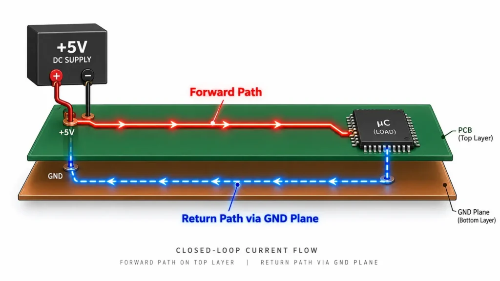
Current must flow in a closed loop. In a simple DC circuit, conventional current may leave the positive terminal of a power source, pass through the load, and return to the source through the conductor labeled GND.
The important phrase is return to the source. Current does not disappear when it reaches a ground symbol. The symbol may replace several drawn wires on the schematic, but the physical conductors, planes, cables, and source connections still form the complete loop.
It helps control noise and EMI
Real conductors have resistance and inductance. Current flowing through ground impedance produces a voltage difference:
V = I Z
For rapidly changing current, parasitic inductance adds a transient component commonly expressed as:
V = L\frac{di}{dt}
This is why “ground” at one PCB location may not be at exactly the same instantaneous potential as “ground” elsewhere. A low-impedance ground structure and compact return paths reduce common-impedance coupling, ground bounce, radiated emissions, and susceptibility to interference.
It can support electrical safety
Protective earth provides a deliberately low-impedance path for fault current so that a fuse, circuit breaker, or other protective device can act. This safety function is different from ordinary signal return. Protective-earth design is governed by the product architecture and applicable electrical-safety standards; it should never be improvised from a generic PCB grounding rule.
How Does GND Work in a Simple Circuit?
Consider a 5 V supply powering a microcontroller:
- The supply creates a potential difference between its 5 V output and return terminal.
- The return terminal is designated as GND.
- Current flows from the supply, through the microcontroller and its support components, and back to the supply through the GND network.
- Signal voltages are interpreted relative to that same GND reference.
If a sensor output is 2 V above the sensor’s ground but the microcontroller’s ground differs by 0.5 V, the receiver may see 1.5 V or 2.5 V, depending on the direction of the offset. That difference can create measurement error or even a logic failure. Good grounding is therefore about both connectivity and the impedance of the return path.
At high frequencies, return current does not simply take one abstract “shortest” path. It divides among available paths according to impedance and tends to concentrate close to the signal trace on its reference plane, where loop inductance is low. A gap or slot in that plane can force the return current to detour, increasing loop area, noise, and radiation.
Common Types of Ground
The word ground can describe several nodes or conductors with different jobs. Their names are useful only when their relationships are clearly defined.
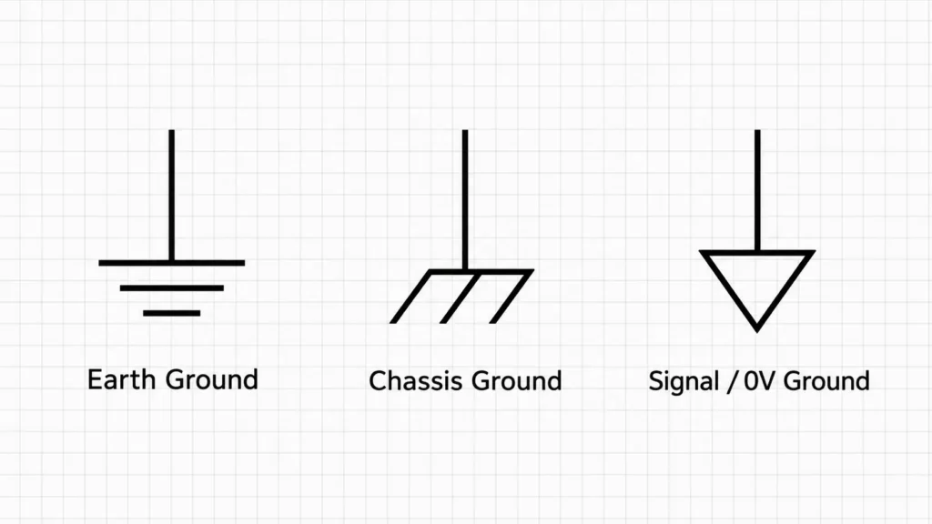
| Ground type | Main purpose | Common use | Important caution |
|---|---|---|---|
| Circuit ground / 0 V | Voltage reference and current return | Most electronic circuits | May float relative to earth |
| Signal ground | Reference and return for signals | Sensors, amplifiers, interfaces | Noise current can corrupt small signals |
| Power ground | Return for higher load current | Motors, converters, power stages | Large current can create voltage drop and ground bounce |
| Analog ground (AGND) | Reference for sensitive analog circuitry | ADCs, DACs, amplifiers | The label does not automatically require a separate plane |
| Digital ground (DGND) | Return for digital switching current | MCUs, FPGAs, logic | Fast edges can generate broadband noise |
| Chassis ground | Connection to a conductive enclosure | Industrial equipment, shielded products | May connect to earth, circuit ground, or both at defined points |
| Protective earth (PE) | Shock and fault protection | Mains-powered equipment | Normally not used as an ordinary load-current return |
| Virtual ground | An actively or passively created reference voltage | Single-supply analog circuits | Has finite current capacity and impedance |
| Floating ground | Local reference with no intentional earth bond | Battery and isolated systems | Can still couple to earth through capacitance or instruments |
National Instruments notes that different ground symbols are not necessarily equivalent and that measurable voltage can exist between grounds. Designers should therefore use the correct symbols and net names instead of placing every ground function on an undefined GND net.
GND vs. Earth, Chassis, and Neutral
These terms are related, but they are not synonyms.
GND vs. earth ground
Circuit GND is an electrical reference chosen within a circuit. Earth ground is an intentional connection to the physical earth or to the protective-earthing system of an installation.
A circuit GND may be:
- directly bonded to protective earth;
- coupled to chassis or earth through capacitors or an impedance network;
- connected at a single controlled point; or
- completely isolated under normal operating conditions.
The correct arrangement depends on shock protection, isolation ratings, ESD, surge, EMI, interfaces, and system-level grounding.
GND vs. chassis ground
Chassis ground connects to a conductive enclosure, frame, shield, or mounting structure. It can provide a path for ESD and high-frequency interference and may also be bonded to protective earth.
Circuit ground and chassis ground are sometimes connected directly, sometimes through a component network, and sometimes kept isolated. Connector shields often need a short, low-inductance path to the chassis rather than a long trace through the signal-ground network. The connection must be planned as part of the product’s EMC and safety architecture.
GND vs. neutral
Neutral is a grounded conductor in an AC power-distribution system and normally carries load current. Protective earth is a safety conductor and normally carries only leakage or fault current. Neither should be treated as a casual substitute for circuit GND.
Neutral and protective earth may be bonded at a defined point in an electrical installation, but connecting them elsewhere can create unsafe touch currents, parallel current paths, or regulatory violations. Mains wiring should be designed and serviced only by qualified personnel under the applicable code.
Is GND Positive or Negative?
GND is neither inherently positive nor negative. It is a reference.
In a typical single-supply digital circuit, the negative terminal of the supply is selected as GND, so the other rail is positive relative to it. However, this is a design choice rather than a universal rule.
Other examples include:
- A split supply may use its midpoint as GND, producing +12 V and −12 V rails.
- Some legacy and specialized systems use a positive-ground architecture.
- A virtual ground may sit at half the supply voltage, such as 2.5 V in a 5 V analog circuit.
- An isolated secondary circuit may have a GND that floats relative to primary-side ground and earth.
Always read the schematic and power architecture before assuming that a terminal marked GND is identical to the supply negative, chassis, or earth.
What Is a Ground Plane on a PCB?
A ground plane is a relatively large copper region connected to a ground net. It may occupy most of an inner PCB layer or appear as a copper pour on an outer layer.
Compared with a long, narrow ground trace, a well-designed plane provides lower resistance and inductance. It also gives high-frequency signal and decoupling currents a compact return path. Texas Instruments and Analog Devices both emphasize the value of low-impedance ground planes for return current, EMI control, and high-speed transmission structures.
Benefits of a continuous ground plane
- Lower return-path impedance
- Smaller signal-current loop area
- Better signal integrity
- Reduced common-impedance coupling
- Lower radiated emissions and susceptibility
- More predictable controlled impedance
- Improved heat spreading in some layouts
A ground plane is not automatically effective just because a large copper area exists. Narrow necks, plane splits, isolated copper islands, sparse stitching vias, and poorly placed antipads can interrupt or constrict the return path.
PCB Grounding Best Practices
There is no single grounding layout that works for every board. A low-frequency sensor, an RF module, a motor controller, and a mains-powered product have different requirements. The following principles provide a useful starting point.
1. Start with current paths, not net names
Identify where each current originates and how it returns to its source. Pay particular attention to switching regulators, clock lines, gate drivers, motors, relays, high-current LEDs, ADC inputs, and communication connectors.
Place and route the circuit so that noisy or high-current loops remain compact and do not share sensitive return paths. Two nets can both be called GND while still interfering with each other through shared impedance.
2. Use a continuous reference plane when practical
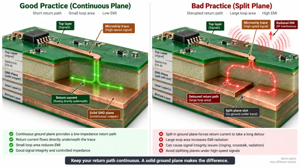
For most multilayer digital and mixed-signal boards, a solid ground plane adjacent to the signal layer provides a dependable reference and short return path. Keep fast traces over the same uninterrupted reference plane for their full route.
Avoid routing a high-speed trace across a split, slot, or void in its reference plane. If the return current must detour around the discontinuity, the larger loop can increase crosstalk and EMI. TI specifically warns that signals crossing a split force return current into large loops.
3. Partition components by function
Physical placement often matters more than assigning multiple ground-net names. Group analog, digital, switching-power, and high-current sections so their local currents circulate within controlled areas.
Keep sensitive analog inputs away from clocks, switching nodes, and fast digital buses. Do not route digital signals through the analog section merely because both regions share one plane.
4. Treat AGND and DGND according to the datasheet
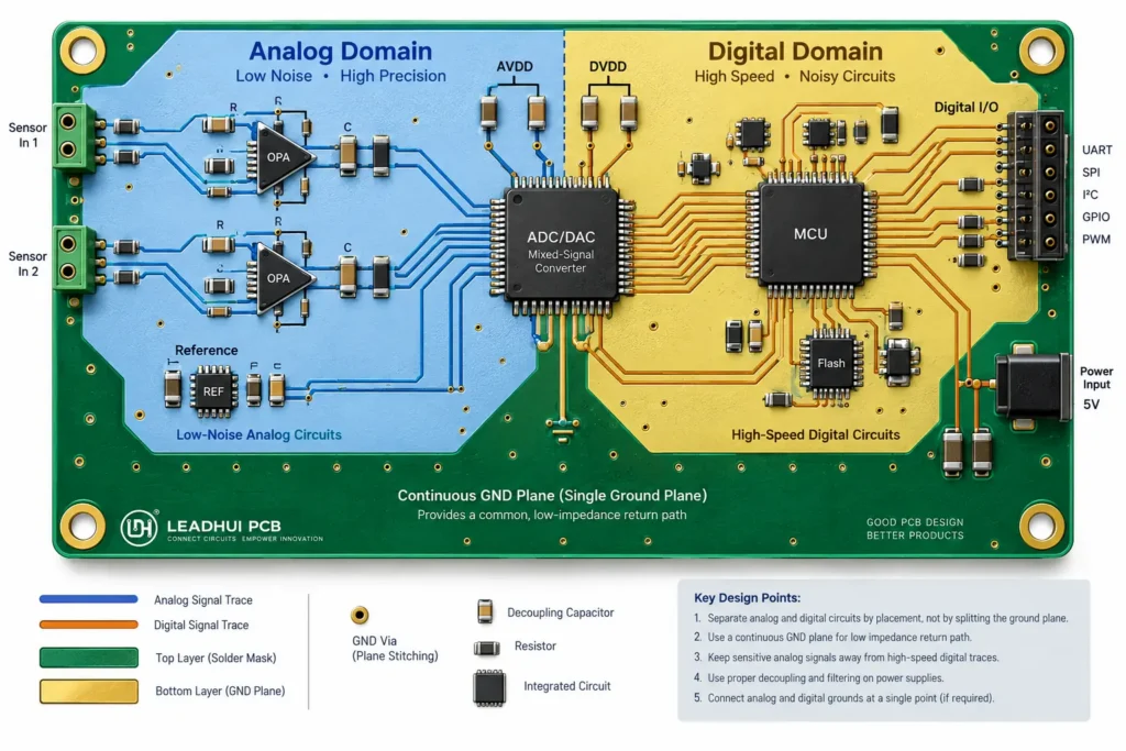
AGND and DGND pins often describe separate functions inside a mixed-signal IC; they do not automatically instruct the PCB designer to create two isolated ground planes. Many converters require both pins to connect to the same low-impedance reference near the device.
Splitting ground without studying return paths can make performance worse. Follow the IC manufacturer’s reference layout, evaluate internal digital current, and verify the design with measurements when the application is sensitive.
5. Keep decoupling loops short
Place each high-frequency decoupling capacitor close to the relevant power and ground pins. Use short, wide connections and place power and ground vias close to the capacitor pads.
The goal is a small, low-inductance loop between the IC, capacitor, power connection, and ground plane. Analog Devices recommends direct connection to a low-impedance plane with short traces or vias because connection inductance reduces decoupling effectiveness.
6. Provide return continuity at transitions
When a high-speed signal changes layers, its return path may also need to move between reference planes. Place ground stitching vias near signal vias when both reference layers are ground. If the signal changes between differently referenced planes, use an appropriate return-path strategy based on the stackup and frequency content.
Stitch ground copper around board edges, shield boundaries, or noisy regions when the EMC design calls for it. Avoid floating copper islands; connect them properly or remove them.
7. Size high-current returns for voltage drop and heat
Motor, heater, LED, battery, and power-converter returns may require wide copper areas, heavier copper, multiple vias, or dedicated planes. Calculate the expected voltage drop and temperature rise rather than assuming that any ground pour is adequate.
Keep these currents out of precision sensor and reference paths. Kelvin connections or separate sense returns may be needed when millivolt-level accuracy matters.
8. Plan chassis and protective-earth connections deliberately
Define where cable shields, chassis, circuit ground, and protective earth connect. Consider fault current, ESD, surge, common-mode noise, isolation, and regulatory clearances. Safety-earth conductors and PCB protective-earth paths must be sized and constructed for their required protective function.
Common GND Mistakes
Assuming every ground symbol represents the same physical node
Schematic symbols reduce clutter, but they can also hide important distinctions. Verify net names and connections between analog ground, digital ground, chassis, isolated grounds, and protective earth.
Splitting the ground plane without a return-path plan
A split may appear to isolate noise while forcing signal return current around a long path. This increases loop area and can create exactly the EMI problem the split was meant to solve.
Routing high current through sensitive ground
If a motor or switching regulator shares a narrow return path with an ADC or sensor, the resulting voltage drop becomes part of the measured signal. Use placement and copper geometry to control where current flows.
Daisy-chaining unrelated ground returns
Connecting several loads in series along one thin ground trace allows the current of one load to modulate the reference of another. A plane, star connection, or carefully partitioned return network may be more appropriate, depending on frequency and current.
Treating ground copper as ideal
Every plane, trace, via, connector, and cable has impedance. At high edge rates, a few nanohenries can matter. Review narrow plane necks, via fields, connector pin assignments, and return transitions—not only DC continuity.
Ignoring test-equipment grounding
The ground clip of many bench oscilloscopes is connected to protective earth. Attaching it to a live, non-earth-referenced node can short that node to earth, damage equipment, or create a shock hazard. Use a properly rated differential probe or isolated measurement method when required.
How to Identify and Test GND on a PCB
Never rely only on trace color, connector position, or a ground-like symbol. Use the schematic, PCB data, component datasheets, and safe measurements.
With power off
- Inspect the schematic for
GND,0V,AGND,DGND,PGND,CHASSIS, andPEnets. - Use continuity or resistance mode to check intended connections.
- Remember that capacitors, semiconductors, filters, or isolation components may prevent a simple continuity result.
- Confirm that separate ground domains are not accidentally shorted by mounting holes, shields, test fixtures, or connectors.
With power on
- Choose the correct reference for the circuit domain being tested.
- Verify that the instrument’s input and ground connection are safe for the expected common-mode voltage.
- Measure DC drop between ground points under realistic load.
- Use an oscilloscope with a short ground spring, differential probe, or suitable probing method to examine high-frequency ground noise.
- Test during switching, communication, motor startup, and other worst-case operating conditions.
Continuity alone cannot prove that a ground system has sufficiently low impedance at the frequencies that matter.
Grounding Checklist Before PCB Fabrication
Use this short review before releasing Gerber and drill files:
- Are all ground domains named and connected intentionally?
- Is the reference plane continuous beneath fast or sensitive signals?
- Do any traces cross a plane split, slot, or large void?
- Are high-current and switching return loops compact?
- Are sensitive analog returns protected from noisy current paths?
- Do AGND and DGND connections follow the component datasheet?
- Are decoupling capacitors close to the correct pins with short via connections?
- Are layer-transition return paths provided where needed?
- Are ground vias sufficient at connectors, shields, and copper-pour boundaries?
- Are ground traces, planes, and vias sized for current and temperature rise?
- Are chassis, shield, and protective-earth connections clearly defined?
- Have isolation distances and safety requirements been reviewed?
- Are test points available for important ground domains and power rails?
For fabrication, provide the final stackup, copper weight, controlled-impedance requirements, current expectations, and any safety or isolation notes. Manufacturing data can reproduce the copper you designed, but it cannot correct an undefined grounding architecture without engineering input.
Frequently Asked Questions About GND
What is the full form of GND?
GND stands for ground. In electronics, it usually identifies the circuit’s reference node and a common current-return network.
Is GND the same as 0 V?
GND is normally assigned a nominal value of 0 V for circuit analysis and measurement. Real ground conductors have impedance, however, so different points on the GND network can develop small voltage differences under load or during fast transients.
Is GND the same as the negative terminal?
Sometimes, but not always. In many single-supply circuits, supply negative is designated as GND. A split supply may use its midpoint as GND, and a positive-ground system may connect GND to the positive terminal.
Does current flow through GND?
Yes, circuit ground commonly carries return current. Protective earth is different: under normal conditions it should not carry ordinary load current, although small leakage current may exist.
Can a circuit work without earth ground?
Yes. Battery-powered and isolated circuits often operate with a floating local GND. They still require a closed current loop and a defined internal voltage reference.
Why do ICs have multiple GND pins?
Multiple pins can reduce connection resistance and inductance, handle current, improve thermal performance, or separate sensitive internal functions. Every required ground pin should be connected according to the manufacturer’s datasheet and recommended layout.
Should analog and digital grounds be separated?
Not automatically. Separate component placement and controlled current paths are usually more important than arbitrary plane splits. Many mixed-signal ICs work best with a common low-impedance ground plane, while some applications require a specific split or single-point connection. Follow the datasheet and analyze the return currents.
What is GND on Arduino and other development boards?
It is the board’s common 0 V reference and power-return connection, usually tied to the negative side of the board’s DC supply. When connecting external modules, their grounds often need to be connected unless the interface is intentionally isolated or fully differential.
What is the difference between VCC and GND?
VCC is a power rail, while GND is the reference and return node. In a 5 V circuit, VCC may be 5 V relative to GND. The names describe different roles; current must travel through both the supply and return portions of the loop.
What causes a ground loop?
A ground loop forms when two points are connected by more than one conductive path, allowing unwanted current to circulate. The resulting voltage drop can introduce hum, measurement error, or EMI. Solutions may involve controlled bonding, differential signaling, isolation, or changes to cable and shield connections.
Conclusion
GND is more than a symbol at the bottom of a schematic. It is the reference that gives circuit voltages meaning and often the network that carries current back to its source. It may be connected to earth, chassis, supply negative, or another reference—but none of those relationships should be assumed without checking the design.
For reliable PCB performance, focus on the physical return path: keep loops compact, preserve continuous reference planes, separate noisy and sensitive current paths through placement, connect decoupling components with low inductance, and follow device-specific guidance for mixed-signal grounding.
If you are preparing a board for production, send LEADHUI PCB your Gerber files, drill data, stackup, copper requirements, and relevant electrical notes for a manufacturability review and PCB quotation.
Technical References
- National Instruments, Chassis, Earth and Signal Grounding: Terminology and Symbols
- Texas Instruments, Grounding in Mixed-Signal Systems Demystified, Part 1
- Texas Instruments, Grounding in Mixed-Signal Systems Demystified, Part 2
- Analog Devices, MT-031: Grounding Data Converters and Solving the Mystery of AGND and DGND
- Analog Devices, MT-101: Decoupling Techniques
