Reflow soldering is the process that attaches surface-mount components to a printed circuit board by heating stencilled solder paste until it melts, wets the component terminations and forms the joint on cooling. It is the primary assembly method for almost every modern electronic product, and it is the step where the most expensive mistakes become permanent.
Most technical guides stop at the oven. They explain the four zones, list the usual defects and finish with a sales page. What they rarely explain is the part that actually decides yield: the profile is built per assembly rather than per oven, the numbers on a paste data sheet and the numbers in a components standard serve different purposes, and a joint is only “good” relative to a named acceptance class.
This guide covers the process from print to inspection, the parameters that govern it, how to validate a profile on a mixed-mass board, and how the common defects map to acceptance criteria rather than to an inspector’s opinion.
Key Takeaways
- The reflow profile is set per assembly, not per oven. Board thickness, copper mass and component mix change how heat arrives, so the same recipe that passes on one product can underheat another.
- Time above liquidus is the parameter that governs joint quality in both directions. Too little leaves incomplete wetting; too much grows an intermetallic layer thick enough to embrittle the joint.
- Published reflow limits differ because they answer different questions. A paste data sheet describes the profile you should run; IPC/JEDEC J-STD-020 describes the worst case a component must survive.
- Most defects are set before the oven. Tombstoning, bridging and warpage trace back to pad symmetry, aperture design and copper balance – layout and stencil decisions no profile can fully offset.
- Lead-free joints are supposed to look dull. Judging a SAC305 joint against the shine of a tin-lead joint is the most common inspection error in the field.
What Is Reflow Soldering?
Reflow soldering is a process in which solder paste, stencilled onto the pads of a printed circuit board, is heated until it melts, wets the component terminations and forms the electrical and mechanical joint on cooling.
The name is literal. The solder arrives as a paste of metal powder suspended in flux, and the joint is formed when that paste reflows: it liquefies, coalesces and solidifies in place. Nothing is fed into the joint during the process. The correct amount of solder was already on the board, or it never will be.
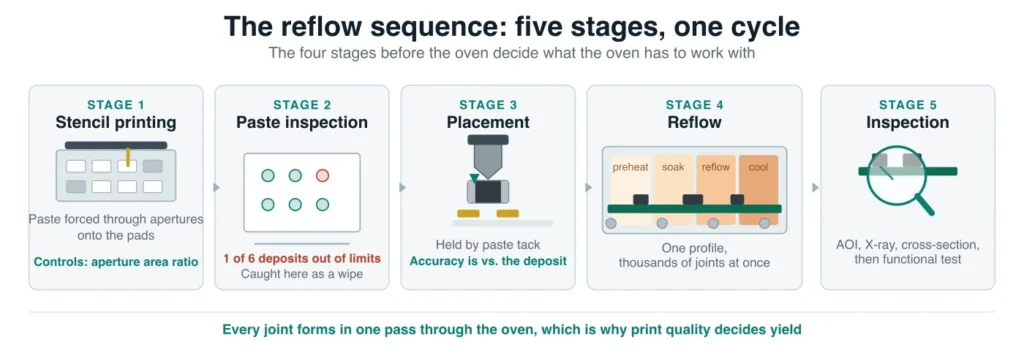
That distinction is what made reflow the default method for surface-mount assembly. Every joint on the board forms in a single thermal cycle, so component count stops being a cost driver in the way it was for hand and wave soldering. Fine-pitch packages, dense boards and double-sided assemblies all become practical when one pass through an oven can join thousands of points at once.
It is worth separating reflow from wave soldering early, because the two are frequently confused. In reflow, solder paste applied to the pads melts where it sits. In wave soldering, the board is passed over a standing wave of molten solder so that solder wicks up through plated holes. Wave remains the high-volume answer for through-hole content; reflow is the answer for surface-mount. Most production boards use both.
This guide is written for the people who have to make the process hold: process engineers qualifying a line, NPI engineers taking a new product to production, quality engineers deciding what to accept, and design engineers whose layout decisions arrive at the printer before anyone else sees them.
How the Reflow Process Works, Step by Step
Reflow soldering is five stages, and the four that happen before the oven decide whether the oven has anything to work with.
1. Stencil printing. A laser-cut stainless steel stencil is aligned to the board, and a squeegee drives paste through the apertures onto the pads. The controlling geometry is the area ratio: the area of the aperture opening divided by the area of its walls. If that ratio is too low, paste adheres to the aperture wall more strongly than to the pad and stays in the stencil instead of transferring. A pad can be starved of solder before the board has moved.
2. Solder paste inspection. An SPI system measures the volume, area, height and alignment of every deposit against limits. This is the cheapest defect gate on the line and the one most often skipped on prototype builds. A print defect caught here costs a wipe. The same defect caught after reflow costs a rework: the part is removed, the site is cleaned and re-pasted, and the joint and the surrounding laminate take another thermal cycle. The gap between those two outcomes is the whole argument for keeping SPI in the line.
3. Component placement. Pick-and-place machines place parts onto the wet paste, which holds them by tack and surface tension until the oven. Placement accuracy is usually quoted by the machine vendor at a stated sigma and component size, but what actually matters is placement relative to the paste deposit. A well-placed part on a misprinted pad is a defect waiting for heat.
4. Reflow. The board is carried through a multi-zone oven and subjected to a controlled temperature profile. The paste melts, the flux activates and burns off its work, the alloy wets the pad and the termination, and the assembly is cooled at a controlled rate. The next two sections take this apart.
5. Inspection. Automated optical inspection checks what can be seen; X-ray checks what cannot; cross-section settles disputes; functional test confirms the product works. Each answers a different question, and the acceptance section explains which one settles the argument.
The Reflow Profile, Zone by Zone
A reflow profile is the temperature the assembly experiences plotted against time. It is set per assembly rather than per oven, because board thickness, layer count, copper distribution and component thermal mass all change how quickly heat reaches a given joint.
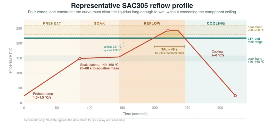
A typical profile has four zones. Each has a purpose, a window, and a specific failure mode when it is wrong.
Preheat
The board is brought from ambient to the soak temperature at a controlled ramp. Its ramp rate exists to limit thermal shock: heating too fast cracks ceramic capacitors and multilayer ceramics, and it spatters the paste, which is where stray solder balls come from. Solvents and volatiles in the paste begin to leave the deposit here.
Indium Corporation’s published reflow limits for SAC305 paste specify an average ramp of 1.0 to 1.5 °C/s, with 0.5 to 2.5 °C/s acceptable (Indium Corporation, SAC305 water-soluble paste data sheet, retrieved 2026-10-21).
Soak
The soak holds the assembly in a temperature band so that everything reaches thermal equilibrium before the peak. This is its real job. Components of different mass heat at different rates, and without a plateau the heavy parts arrive at the peak late while the light parts are already past it.
Soak is also where flux does its chemistry: it reduces the oxides on the pad and the termination so the alloy can wet them. Run the soak too long or too hot and the flux is consumed before the alloy melts. The result shows up as graping, where the solder particles fail to coalesce into a single mass, and as head-in-pillow, where a BGA ball and its paste never merge.
Reflow
The assembly is taken above the alloy’s liquidus so the solder melts, wets both surfaces and forms the metallurgical bond. What governs here is time above liquidus, usually abbreviated TAL: the number of seconds the joint spends molten.
TAL is a two-sided constraint. Too little time and the alloy does not fully wet the pad and the termination, which produces a weak or intermittent joint. Too much time and the intermetallic layer between the solder and the copper grows thicker than it needs to be, which leaves the joint more brittle than the bulk alloy predicts. Separately, the peak is capped by what the components can survive.
Indium’s SAC305 data sheets specify 45 to 60 seconds above liquidus as recommended, with 30 to 100 seconds acceptable, and a peak of 230 to 260 °C. SAC305 is not a true eutectic: it melts over a narrow range, with a solidus of 217 °C and a liquidus of 220 °C (Indium Corporation, alloy data for Indalloy 256, retrieved 2026-10-21). Both windows are anchored to the liquidus rather than chosen in isolation. The peak band sits 10 to 40 °C above it – the floor set by the alloy, the ceiling by what the components will survive – while the TAL window is the time the alloy spends above that line.
Cooling
Cooling solidifies the joint and sets its grain structure. It is the most neglected zone on the profile, and the one where two legitimate concerns pull against each other.
Indium’s data sheets recommend 2 to 6 °C/s with 0.5 to 6 °C/s acceptable, noting that faster cooling promotes a finer grain structure. The opposing concern is thermal stress. Ceramic capacitors and the laminate itself are damaged by a steep temperature gradient, which is why some assemblers cap the cooling slope well below the paste window’s upper bound. Both effects are real. Cool too slowly and the grain coarsens while intermetallic growth continues; cool too fast and the parts and laminate take a shock they were not qualified for.
There is no universal number that resolves it. The paste data sheet sets the window the alloy tolerates. The component data sheet sets the gradient the package tolerates. The assembly’s thermal mass sets what the oven can physically deliver. Where those conflict, the component limit governs, because that is where the damage is irreversible.
RSS vs RTS: Choosing a Profile Shape
Two profile shapes cover most production work, and the choice is governed by how uneven the thermal mass on the board is.
| Property | Ramp-soak-spike (RSS) | Ramp-to-spike (RTS) |
|---|---|---|
| Shape | Ramp, plateau, spike, cool | Continuous ramp, peak, cool |
| Thermal uniformity | High, because the plateau equalises | Lower, because light parts lead |
| Process time | Longer | Shorter |
| Best for | Mixed thermal mass, dense assemblies, large boards | Simple boards with uniform mass |
| Main risk | Flux exhaustion if the soak runs long | Cold joints on heavy parts, voiding |
RSS holds the assembly at a plateau so that heavy and light components arrive at the peak together. RTS removes the plateau and runs a single ramp, which is faster and consumes oven time efficiently but leaves more thermal spread across the board.
Most production assemblies with a genuinely mixed component mix end up on a soak profile. If a board carries both a 01005 passive and a large power inductor, the plateau is what stops one from being overfired while the other is underfired.
How to Build and Validate a Reflow Profile
Build the profile from the paste data sheet, not from the oven’s saved recipe. The paste defines the window; the oven is adjusted to fit inside it. Validation then proves that the assembly, not just the paste, stays in that window.
1. Read the constraints off the data sheet. Ramp rate, soak band and duration, peak range, TAL and maximum peak temperature. These are the limits. Everything that follows is adjustment within them.
2. Set the component ceiling. The lowest maximum body temperature among the parts on the board caps the peak, and reflow classification for moisture-sensitive packages is defined in IPC/JEDEC J-STD-020. A profile that satisfies the paste but exceeds a component’s classification temperature is still wrong, and the failure may not appear until the product is in the field.
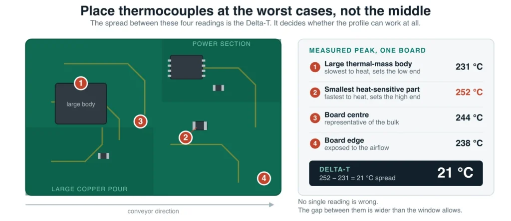
3. Attach thermocouples to the worst cases, not to the middle. Place them on the largest thermal mass component, the smallest and most heat-sensitive part, the centre of the board, and the board edge. Add one under a BGA where it can be done. The centre-to-edge spread of these readings is the Delta-T, and it is the single number that tells you whether the profile is viable.
4. Run the profile and read the Delta-T. If the spread across the board exceeds what the process window allows, the profile is not yet finished regardless of whether each individual thermocouple looks acceptable.
5. Close the Delta-T gap in a fixed order. Conveyor speed first, because it shifts the whole curve in time without changing zone relationships. Then zone setpoints, which change the shape. Then zone boundaries, and only if the first two cannot close it. Changing several at once makes the result uninterpretable.
6. Record and control it. Store the profile against board revision, paste lot and date. Re-profile when the paste changes, the stackup changes, the component mix changes, after oven maintenance or repair, and on a periodic interval as part of process control. A profile you cannot reproduce is not a control; it is a coincidence.
The Delta-T problem is the one that catches NPI engineers, and it is worth stating plainly. On a board with a small, dense logic section and a large ground-poured power section, the two areas can run tens of degrees apart through the peak. You cannot fix that by raising the peak, because the light area was already at its limit. You fix it by slowing the ramp, extending the soak so the heavy area catches up, or changing the board: adding thermal relief, balancing copper, or moving the heavy components together.
Reflow Temperatures by Solder Alloy
The reflow window follows the alloy’s liquidus temperature. The peak is set far enough above liquidus to guarantee complete melting and wetting, and no further than the components will tolerate.
| Alloy | Composition | Solidus / liquidus | Typical peak | Typical TAL | Notes |
|---|---|---|---|---|---|
| SAC305 | Sn 96.5 / Ag 3.0 / Cu 0.5 | 217 / 220 °C | 230 to 260 °C | 45 to 60 s recommended | Production baseline for lead-free work |
| Sn63/Pb37 | Sn 63 / Pb 37 | 183 °C (eutectic) | about 210 to 220 °C | 30 to 60 s | Wider process window; permitted only under a RoHS exemption |
| Sn42/Bi58 | Sn 42 / Bi 58 | 138 °C (eutectic) | about 165 to 180 °C | per paste data sheet | For heat-sensitive parts and second-pass reflow |
Two things about this table matter more than the numbers themselves.
J-STD-020 and a paste data sheet are not describing the same thing. IPC/JEDEC J-STD-020 defines the moisture sensitivity classification of plastic surface-mount packages, and its Pb-free test profile runs a soak of 150 to 200 °C for 60 to 120 seconds, 60 to 150 seconds above 217 °C, and a classification peak of up to 260 °C. That is the worst case a component is required to survive on the bench, repeated across cycles. It is not a recommendation for what to run on your board. Confusing the two is how engineers end up running profiles far hotter and longer than the paste needs.
Mixed-alloy assemblies are a process decision, not a materials detail. Lead-free paste on a board with a leaded surface finish, or the reverse, changes the joint’s composition at the interface. The result may be acceptable, but it should be a documented decision with a rationale, not an accident of what was in stock.
Legacy tin-lead work remains lawful only within the exemptions in the EU Restriction of Hazardous Substances Directive (2011/65/EU), which restricts lead in electrical and electronic equipment subject to a published list of exemptions (European Commission, RoHS Directive, retrieved 2026-10-21). Do not assume an exemption applies to your product; check the current list.
Solder Paste Selection and Handling
Solder paste is metal powder suspended in flux and a vehicle system, and the powder size type is chosen by the finest pitch on the board rather than by preference or price.
Powder size. IPC J-STD-005 classifies solder powder by particle size, and the classification is based on the proportion of particles falling inside a nominal range. Finer powder prints finer apertures, but it carries more surface oxide per unit mass, is more prone to voiding, and has a shorter stencil life. The working rule is to choose the coarsest type that clears the finest pitch on the board.
| Powder type | Particle range | Typical application | Trade-off |
|---|---|---|---|
| Type 3 | 25 to 45 µm | Standard pitch, 0.5 mm and above | Best stencil life, least voiding |
| Type 4 | 20 to 38 µm | Fine pitch, about 0.4 to 0.5 mm | Balanced; the common fine-pitch choice |
| Type 5 | 15 to 25 µm | Very fine pitch, 0.3 mm and below | Finest print, highest oxide load, shortest life |
Flux chemistry. No-clean, water-soluble and rosin fluxes differ in activity and in residue. The choice is made at the printer and paid for later: at conformal coating, at cleanliness testing, or at a field failure that traces back to residue under a component. If the assembly will be coated, confirm compatibility with the coating supplier before the paste is qualified, not after.
Metal load and viscosity determine how the paste behaves through the aperture and how long it survives on the stencil. They are print-quality variables, not constants, and they change with temperature and with time on the stencil.
Storage and handling. Paste is normally stored refrigerated and must be brought to room temperature before use, because a cold deposit condenses moisture and prints unevenly. Stencil life is finite and stated by the manufacturer. Paste that has been open too long prints differently from paste that has not, and the difference shows up as volume variation that SPI will catch and nobody will believe.
Reflow Equipment and How to Specify It
Three heating technologies divide the market, and choosing between them is a trade between uniformity, thermal mass capability and cost rather than a question of which is newest.
Forced convection, infrared and vapour phase
Forced convection is the production default. Heated air is circulated across multiple independently controlled zones, and because the air is physically blown across the board, it transfers heat by convection to every exposed surface regardless of the part’s colour, material or finish. That is what makes it uniform across a mixed board. The number of zones is a resolution specification, not a quality one: more zones let you shape the curve more finely, they do not make the joint better.
Infrared heating transfers energy by radiation. It is efficient and mechanically simple, but different materials absorb at different rates, and shadowing means a large component can shield the area behind it. That is why IR is now more common in benchtop and rework equipment than in production lines.
Vapour phase immerses the assembly in a saturated vapour of an inert perfluorinated fluid, which condenses on the board and transfers latent heat at a fixed temperature set by the fluid’s boiling point. Heat transfer is extremely uniform, which suits high thermal mass and heat-sensitive parts, and the vapour displaces oxygen so oxidation is limited. The trade-offs are fluid cost, fluid handling and a batch rather than continuous process for many systems.
Nitrogen and vacuum
Nitrogen inerting reduces oxidation during reflow and improves wetting, which matters most for fine-pitch packages, lead-free alloys and high-reliability products. It is a running cost, so the decision is whether the defect reduction pays for the gas. For a mature, well-controlled line making simple boards, it often does not. For fine-pitch BGA and QFN work in automotive or medical products, it usually does.
Vacuum reflow applies a vacuum while the alloy is molten, drawing trapped gas out of the joint and reducing voiding substantially. It is the strongest available lever on voids in bottom-termination and array packages, and it is a capital decision rather than a profile adjustment.
Sizing an oven for your throughput
Oven sizing, worked through
An assembler needs 180 boards per hour. Each board is 8 inches long, and the paste manufacturer recommends a four-minute, three-step profile. The conveyor allows a 2-inch gap between boards, so the load factor is 0.8.
Step 1. Boards per minute. 180 / 60 = 3 boards per minute.
Step 2. Required line speed. (3 boards/min × 8 in/board) / 0.8 = 30 inches per minute.
Step 3. Required heated length. 30 in/min × 4 min = 120 inches, or 10 feet.
The oven needs at least 120 inches of heated length. Overall length will be greater, because the cooling section, the load section and the unload section sit outside the heated zones. Quoting on overall length instead of heated length is a common and expensive misunderstanding.
Designing the Board for Reflow
Most reflow defects are designed in before the board reaches the printer. Tombstoning, bridging and warpage each trace back to a specific layout or stencil decision.
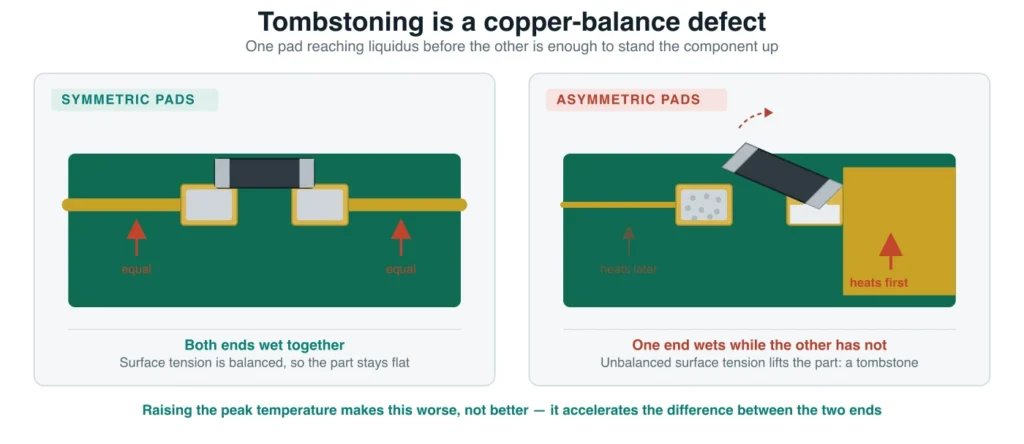
Thermal symmetry across a component’s pads is the tombstoning mechanism. If one pad has a large copper connection and the other has a thin trace, one end of the component reaches liquidus before the other. The first end wets, surface tension pulls, and the part stands up. Fix the copper balance on the two ends and the defect largely disappears.
Copper balancing across a panel governs warpage. Large unbalanced copper areas heat and expand unevenly, and the panel bows as it passes through the peak. The remedy belongs in the waste area of the panel, where copper is added to equalise the distribution, not on the board itself.
Component orientation relative to conveyor travel matters for long parts. Placing elongated components across the airflow rather than along it reduces the chance of the part being lifted or shifted while the alloy is molten.
Pad geometry and spacing control bridging. Solder bridging is a paste volume and spacing problem, not an oven problem, and it is corrected at the stencil rather than at the profile.
Edge rails and keep-outs give the conveyor something to clamp and stop components or paste being disturbed at the board edge during transport.
Stencil aperture rules by package do most of the remaining work:
- Rounded aperture ends on fine-pitch devices, to reduce stress concentration and improve paste release.
- Square apertures for BGA pads and ultra-miniature passives, to give uniform deposit and predictable ball formation.
- Cross-shaped apertures on QFN thermal pads, to control the paste volume under a large exposed pad and reduce solder beading at the edges.
- Aperture reduction on fine-pitch devices, where bridging is driven by excess volume rather than by spacing.
Fiducials give the placement machine a reliable datum. Without them, placement accuracy is limited by the board’s fabrication tolerances and panel registration rather than by the machine.
Via-in-pad without filling wicks paste down the barrel during reflow, starving the joint and contaminating the opposite side. If vias must sit in a pad, they need to be filled and capped, and the fill type should be specified by reference to IPC-4761, Design Guide for Protection of Printed Board Via Structures, which defines the via protection types and their acceptance. That is a fabrication decision made before the board is ordered.
Double-Sided and Mixed-Technology Assemblies
Most real products are not all surface-mount. The decision about how to handle the through-hole content, and how to sequence a two-sided build, is live on every new assembly.
Second-pass reflow
On a double-sided board the first side is reflowed, then the board is flipped and the second side is printed, placed and reflowed. The problem is that the first side’s joints are exposed to a second thermal cycle and the alloy softens above its solidus.
Practical rules reduce to sequencing and mass. Solder the side with fewer or smaller components first, so the heavy parts are on the second pass where they are not at risk of falling. Where heavy parts must be on the first side, adhesive dots hold them through the second reflow. The second pass is usually run at a slightly lower peak, and in some designs a thermal shield protects the underside.
Through-hole parts on a reflow line
Most mixed-technology work uses one of three options:
| Process | Best board mix | Volume band | Main constraint |
|---|---|---|---|
| Pin-in-paste | Through-hole parts on an otherwise SMT board | Low to high | Paste must fill the barrel as well as the joint, so apertures and deposits are larger |
| Selective soldering | Mixed boards with a modest through-hole count | Low to medium | Nozzle access and cycle time per joint |
| Wave soldering | Dedicated through-hole or mixed boards | High | Masking or fixturing for the SMT side |
Pin-in-paste is the option most worth understanding, because it removes a whole process step. Paste is printed over the through-hole pads with apertures enlarged to deposit enough volume to fill the barrel as well as form the fillet, the components are placed, and the whole assembly reflows in one pass. Volume is the constraint: the deposit has to supply the joint and the barrel, which forces larger apertures and a taller paste deposit than the same pad would take for a surface-mount part.
The decision rule is content and volume. Through-hole count drives the process choice, not preference, and most boards end up using more than one process on the same assembly. Pretending otherwise is how quotations go wrong.
Common Reflow Defects and What Causes Them
Reflow defects are not random. Each common one has a short list of causes, and those causes are process parameters you can measure or layout decisions you can inspect.
| Defect | Appearance | Governing cause | Correction | Acceptance class |
|---|---|---|---|---|
| Tombstoning | One end of a chip component lifts and stands vertically | Thermal imbalance across the pads, uneven paste volume, or an over-fast ramp | Balance pad copper, equalise deposit, slow the ramp | Class 2 and Class 3: rejectable where the termination is lifted clear of the pad |
| Bridging | Solder joins adjacent pads or leads | Excess paste volume, aperture design, poor stencil gasketing | Reduce aperture size, adjust print pressure, verify alignment | Class 2 and Class 3: rejectable where the bridge is a short between conductors |
| Voiding | Gas pockets inside the joint, most often in BGA, QFN and power packages | Outgassing, oxide, paste handling, ramp rate | Use low-voiding paste, extend preheat, consider vacuum or nitrogen | Class 3 is stricter; assess against the applicable criteria and any agreed void limit |
| Head-in-pillow | BGA ball sits on the paste without coalescing | Warpage of package or board at reflow, aggravated by oxidation | Increase paste, use a more oxidation-resistant flux, adjust the profile, use an inert atmosphere | Class 3: rejectable, because the joint is not metallurgically formed |
| Graping | Granular, oxidised surface resembling a cluster of grapes | Flux exhausted before the alloy coalesced, through excessive soak or TAL | Shorten soak, reduce TAL, use more thermally stable paste | Rejectable as insufficient wetting |
| Solder balling | Small spheres scattered around pads or traces | Paste spatter from too fast a ramp, poor stencil cleaning, degraded paste | Slow the preheat, clean the stencil, control paste life | Depends on size and location; assess against the applicable criteria |
| Cold or disturbed joint | Dull, rough or fractured fillet | Insufficient peak or TAL, or vibration while molten | Verify the profile against the paste data sheet, stabilise the conveyor | Rejectable as insufficient wetting |
| Component shift or skew | Part displaced from its pad during reflow | Imbalanced wetting, conveyor vibration, or airflow disturbance | Balance paste, stabilise transport, review fan settings | Assess against placement criteria |
| Warpage | Board or panel bows through the peak | Copper imbalance, asymmetric stackup, moisture | Balance copper, review stackup, bake before reflow | Process indicator or defect depending on the resulting joint condition |
| Popcorning | Cracking or delamination from absorbed moisture flashing at peak | Moisture absorbed before reflow in a moisture-sensitive package | Bake to the schedule in IPC/JEDEC J-STD-033, control floor life | Defect: the package has been damaged |
Voiding and head-in-pillow defeat the same assumption: that a joint which looks made is made. Tombstoning belongs on this list for a different reason. It is visible enough, but the imbalance is built into the pad copper, so slowing the ramp can soften it while the durable fix is a layout or stencil change.
Voiding in array packages is the defect where profile changes do the least work. Voids form when gas cannot escape before the alloy solidifies, so the levers are ramp rate, paste chemistry, preheat duration and atmosphere. In a BGA or QFN the gas has a long path out, which is why these packages void more than gull-wing parts. Vacuum reflow is the strongest single intervention; low-voiding paste and a longer, gentler preheat are the cheaper ones.
Head-in-pillow is the defect that most often survives inspection, because the joint looks made from above. Warpage is the mechanism: a package that bows during reflow lifts its balls out of the paste, and by the time it flattens again the paste has already reflowed without them. Indium Corporation’s technical work on the defect attributes it to component or board warpage at reflow, aggravated by oxidation, and recommends solder paste as the most practical countermeasure (Indium Corporation, Testing and Prevention of Head-In-Pillow, retrieved 2026-10-21). Detection usually requires X-ray or a dye-and-pry test, which is why first-article work on a BGA board should include one.
Tombstoning is the clearest example of a defect that is designed in. The published mitigation is pad symmetry and consistent paste volume, both of which are layout and stencil decisions. Raising the peak temperature to “make sure it wets” makes tombstoning worse, not better, because it accelerates the difference between the two ends.
Inspection and Acceptance Criteria
Inspection answers whether the process worked. Acceptance answers whether the result is good enough. Those are different questions, and they are answered by different standards.
In sequence, the gates are: SPI before reflow, checking paste volume and alignment; AOI after reflow, checking presence, polarity, alignment and visible joint form; X-ray for joints that cannot be seen, which in practice means BGA, QFN and other bottom-termination packages; cross-section for destructive verification when X-ray is ambiguous and the question is serious; and functional test as the final product-level gate.
Acceptance is a separate layer. A joint is judged against a named standard and a named class, not against an inspector’s eye. That standard is IPC-A-610, Acceptability of Electronic Assemblies, currently at Revision J, published in 2024 and superseding Revision H. Its criteria are organised by product class, where Class 1 covers general electronics, Class 2 covers dedicated service electronics, and Class 3 covers high-performance and harsh-environment products.
Two consequences follow in practice.
Class is a commercial decision made before production, not a judgement at the bench. Choosing Class 3 for a product whose environment does not demand it buys inspection cost without buying reliability. Choosing Class 2 for a product that will see thermal cycling in a vehicle buys a warranty problem.
Lead-free joints are supposed to look different. A SAC305 fillet is typically duller, grainier and more rounded than the bright, concave tin-lead fillet that many inspectors were trained on. Judging a lead-free joint by its shine is a legacy criterion and it produces both false rejects and, worse, false confidence when a genuinely defective joint happens to be shiny.
Behind every criterion in that standard sit three condition states: Acceptable, Process Indicator and Defect. The middle one is where most arguments happen. A Process Indicator is a condition that is not ideal but does not compromise form, fit or function at the stated class, so it is not a reason to reject a board. Treating every Process Indicator as a defect drives rework that introduces more risk than the original condition carried, and on a Class 3 product it also drives cost that the specification never asked for.
How to Qualify a Reflow Process
Qualifying a reflow process means proving, on paper, that it is in control before production runs. The deliverable is a first-article record, not a good-looking board.
- Profile captured. First-article profile recorded, with every thermocouple reading and the Delta-T stated.
- Paste traceability. Alloy, lot, powder type and date recorded against the profile they were run on.
- SPI limits. Volume and alignment limits set and documented for this specific assembly.
- AOI coverage. The programme tuned to the defect set this assembly actually produces, not left on a default.
- Hidden joints. An X-ray sampling plan defined, including a first-article check on any array package.
- Records. Profile stored against board revision, paste lot and date.
- Re-profile triggers. Written down and owned by a named role.
- Acceptance class. Recorded in writing, with the standard number and revision letter.
- Rework. Criteria and a permitted rework-cycle count defined, including how reworked joints are re-inspected.
- Moisture sensitivity. Components identified, with bake and floor-life controls in place.
Frequently Asked Questions
What is the difference between flow soldering and reflow soldering?
In reflow soldering the solder arrives as paste applied to the pads and melts where it sits. In flow, or wave, soldering the board is passed over a standing wave of molten solder which wicks up through plated through-holes. Reflow is used for surface-mount content and wave for through-hole content, and many production boards use both processes.
Can I use a heat gun to reflow solder?
Yes for removing or replacing a single component, and no for building a board. A heat gun has no controlled ramp, no soak and no measurable peak, so it cannot deliver a profile and cannot produce a repeatable joint. It is a rework tool, and even in rework it risks delaminating the laminate and overheating adjacent parts.
How do you reflow solder at home?
The realistic routes are a hot plate, a converted toaster oven or a hot-air station. None of them gives zone control or a measured profile, so you cannot verify time above liquidus or peak temperature, and you have no acceptance criteria beyond whether the joint looks joined. For prototype work where the board is not safety-critical, that is a reasonable trade. It is not a substitute for a controlled process.
What is type 4 solder paste?
Type 4 is a powder size classification under IPC J-STD-005, spanning 20 to 38 µm, and it is the common choice for fine-pitch work around 0.4 to 0.5 mm. Choose the coarsest type that clears the finest pitch on the board, because finer powder prints better but oxidises faster and reduces stencil life.
What is the ideal reflow soldering temperature?
There is no single temperature, because the peak is set by the alloy and capped by the components. For SAC305, which melts between 217 and 220 °C, a peak of 230 to 260 °C is the published range, with 45 to 60 seconds above liquidus recommended. The upper bound is set by the lowest maximum body temperature among the parts on the board.
Why do my lead-free solder joints look dull?
Because SAC305 joints are normally dull and grainy. The bright, concave fillet that many inspectors associate with a good joint is characteristic of tin-lead alloys. Judging a lead-free joint by its shine is a legacy criterion, and it is the most common inspection error in lead-free assembly.
How often should a reflow profile be revalidated?
Re-profile whenever the paste changes, the stackup changes, the component mix changes, or the oven has been maintained or repaired, and on a periodic interval as part of process control. A profile stored against a board revision but not against a paste lot is an incomplete record, because a paste change alone can move the result.
Where to Start
Check two things about your own process before changing anything. First, whether your profile was validated against the assembly you are actually running, or inherited from a similar board. Second, whether your acceptance class is written down and cited with the standard revision, or assumed.
If the profile is inherited, the fastest improvement is usually not a new oven setting. It is a Delta-T measurement on the current board, because that tells you whether the profile is even capable of working across the assembly. If the class is assumed, the cheapest improvement is to name it in writing on the next purchase order, which costs nothing and removes an argument that otherwise surfaces at final inspection.
Both checks cost almost nothing and both are things a supplier will answer directly if asked. A profile question should produce a chart with thermocouple traces and a board revision on it. A class question should produce a name, a revision letter and a date. Anything vaguer than that is worth treating as unverified.
Sources
- Indium Corporation, SAC305 water-soluble solder paste product data sheet, for the recommended and acceptable ramp rate, soak window, time above liquidus, peak temperature and cooling rate. Retrieved 2026-10-21.
- Indium Corporation, solder alloy data for Indalloy 256 (SAC305), for the 217 °C solidus and 220 °C liquidus. Retrieved 2026-10-21.
- Indium Corporation, Testing and Prevention of Head-In-Pillow, technical paper, for the warpage and oxidation mechanism of head-in-pillow and the recommended countermeasures. Retrieved 2026-10-21.
- IPC / Global Electronics Association, Meet Your Standards, for the scope of IPC-A-610, J-STD-001 and the related standards family. Retrieved 2026-10-21.
- IPC, IPC-A-610J: Acceptability of Electronic Assemblies, published 2024, superseding Revision H (2020). Available through IPC and its licensed resellers, including the ANSI Webstore.
- IPC/JEDEC, J-STD-020: Moisture/Reflow Sensitivity Classification for Nonhermetic Solid State Surface Mount Devices, for the Pb-free classification profile limits and the classification peak temperature.
- IPC, J-STD-005: Requirements for Soldering Pastes, for the solder powder particle size classification, including Type 3 (25 to 45 µm), Type 4 (20 to 38 µm) and Type 5 (15 to 25 µm).
- IPC/JEDEC, J-STD-033: Handling, Packing, Shipping and Use of Moisture/Reflow Sensitive Surface Mount Devices, for the bake schedule and floor-life controls referenced in the moisture section.
- IPC, IPC-4761: Design Guide for Protection of Printed Board Via Structures, for the via protection types referenced in the board design section.
- European Commission, RoHS Directive, for the restriction on lead in electrical and electronic equipment and the exemption mechanism. Retrieved 2026-10-21.