Eine HDI-Leiterplatte, or high-density interconnect printed circuit board, uses fine conductors and compact interlayer connections to fit more wiring into a given area. Laser-drilled microvias and thin buildup layers help connect dense component pads without using a full-thickness hole at every connection.
The design question is whether those features solve a routing constraint worth the added processing. Start with package geometry and layer access, then compare constructions. A small pitch alone cannot choose the stackup.
Wichtige Erkenntnisse
- HDI describes interconnect density and construction; adding layers alone does not make a board HDI.
- Ball grid array (BGA) pitch, copper pad size, trace clearance and via lands jointly constrain escape routing.
- A trace fitting between two pads does not prove that the whole package can escape.
- Compare candidate stackups on processing, total board cost and reliability evidence before releasing fabrication files.
What Makes a PCB High Density?
HDI construction increases usable routing space through smaller interconnect features. A microvia can connect a surface layer to the next copper layer while leaving deeper layers available for other routes. Fine traces and small capture pads provide additional escape paths around dense packages.
Sierra Circuits’ HDI design reference describes the combination of higher wiring density, microvias, material selection and buildup planning. Its dimensional examples describe particular design conditions; use your fabricator’s approved rules for the actual construction.
Keep three distinctions clear:
- Lagenanzahl tells you how many copper layers are available.
- Via span tells you which layers an interconnect joins.
- Feature dimensions tell you what routing and registration tolerances the process must support.
An ordinary multilayer board can have many layers and large through-holes. An HDI board can have fewer layers but more demanding interconnections. Likewise, high signal speed does not by itself require HDI. Electrical performance still depends on material, impedance, reference planes and the routed geometry.
HDI PCB vs Standard PCB: When Is It Justified?
Choose HDI when conventional routing cannot satisfy the package, board-area or connection requirements within an acceptable construction. Compare both options before assuming that a denser process is necessary.
| Design constraint | Conventional through-hole construction | HDI construction |
|---|---|---|
| Escape around dense component pads | Drill and land size may block routing channels | Smaller microvia lands can open useful routes |
| Access to an adjacent layer | A through-hole occupies space through the board | A blind microvia can stop at that layer |
| Limited board area | More routing layers or a larger outline may be needed | Buildup routing may help retain the outline |
| Manufacturing effort | Fewer process stages for a simple construction | Additional lamination, drilling and plating may be required |
| Total cost | Often attractive when routing already fits | Depends on whether area or layer savings offset extra processing |
A shorter interconnect can help electrical design, but an HDI label does not guarantee signal integrity. Check transitions and return paths with the same care as trace impedance. The controlled impedance and reference-plane guide develops those checks.
HDI PCB Stackup: 1+N+1, 2+N+2 and Any-Layer
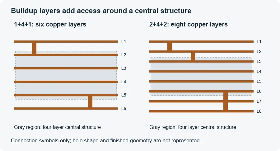
Buildup notation describes added copper layers around a central structure. It helps compare architectures, but it does not fully specify their via connections or manufacturing sequence.
Read the buildup notation
In 1+N+1, one buildup copper layer sits on each side of an N-layer central structure. A 1+4+1 construction therefore has six copper layers. A 2+4+2 construction has eight.
The central structure can contain its own connections, including buried vias. Total factory press operations depend on how that structure and the added layers are made. Do not equate the notation with an exact count of every lamination operation.
Altium’s HDI design and manufacturing explanation connects buildup, layer planning and manufacturing capability. Agree the detailed layer and via-span drawing with the fabricator before routing to it.
Separate via arrangement from via location
Stacked microvias align over one another across successive layer pairs. Staggered microvias are offset, with a conductor joining their landing areas on the intermediate layer. Staggering consumes routing area; stacking places greater demands on the supporting filled structure and its interfaces.
Via-in-Pad describes location: the via opening lies within a component land. It does not specify the fill material or finished surface. Laser microvias may be copper filled; larger through-vias can use a different filling and capping process. Specify the required finished structure so the pad supports assembly without unintended solder loss into the opening.
Any-layer HDI, also called every-layer interconnect (ELIC), makes connections between arbitrary copper layers available through copper-filled stacked microvia structures. Sierra Circuits’ HDI manufacturing reference describes this architecture. Unlike the central-structure examples above, microvia connectivity extends throughout the layer structure. Each net still connects only to its assigned conductors; any-layer does not mean electrically joining every layer on every net.
Sierra’s design reference also describes stacked and staggered arrangements. Select the architecture with the fabricator using the actual escape requirement. The PCB via types and design rules cover spans, filling and capping in greater detail.
Worked Example: Can a Trace Escape Between These BGA Pads?
A trace can pass between adjacent pads only if their copper-to-copper gap accommodates its width and clearance on both sides. That local check is useful before comparing stackups, but it cannot establish a package’s total escape capacity.
State the geometry
Consider a teaching example with these nominal dimensions:
| Input | Assumption |
|---|---|
| Ball pitch, measured between pad centers | 0.50 mm |
| Circular copper pad diameter | 0.25 mm |
| Candidate trace width | 0.075 mm |
| Candidate trace-to-pad clearance | 0.075 mm |
These values are illustrative, not a component recommendation or a LeadPCB capability guarantee. The pad dimension is copper diameter, not solder-mask opening. The calculation excludes fabrication compensation, registration allowances and process tolerances.
Calculate one channel
The gap between the copper edges is:
Gap = pitch − pad diameter = 0.50 − 0.25 = 0.25 mm.
One trace needs:
Required gap = trace width + 2 × clearance = 0.075 + 2 × 0.075 = 0.225 mm.
The nominal geometric margin is 0.025 mm. That is the unused width across the whole gap, not a tolerance allowance assigned to either edge. A 0.10 mm trace with 0.10 mm clearance needs 0.30 mm and therefore fails this same nominal check.
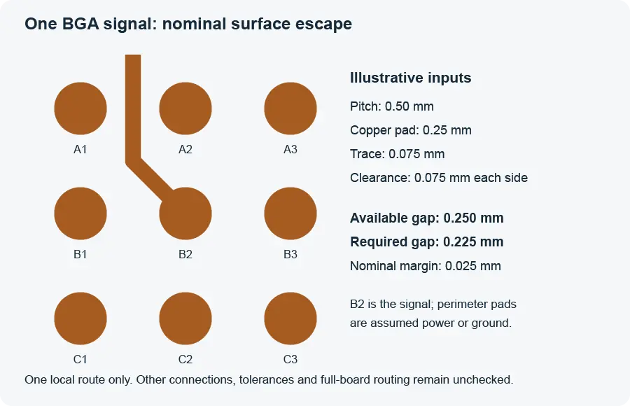
To make the routing task concrete, assume a small illustrative 3×3 pad array: A1–A3 on the top row, B1–B3 in the middle and C1–C3 on the bottom. Assign the center pad B2 to one signal and the eight perimeter pads to power or ground. This deliberately simplified ball map is not a commercial package.
A possible local route leaves B2 upward between A1 and A2, then exits the array. The diagram shows that one signal’s path through one channel. Power distribution, solder-mask constraints, the other pads’ connections and the complete board layout remain unresolved. A larger, fully populated signal array would present a different escape problem.
Compare candidate constructions
| Candidate | What it could solve | What remains to confirm |
|---|---|---|
| Conventional through-hole board | Keep the illustrated signal on the surface and place transitions outside the array | Full ball map, remaining routes, power distribution and allowed trace rules |
| 1+N+1 | Move selected pads from the surface to an adjacent layer using microvias | Capture lands, dielectric depth, clearances and routing capacity on that layer |
| 2+N+2 | Provide another buildup routing level where a completed escape study needs it | Connections across both buildup layers, via arrangement and additional processing |
For the one illustrated signal, the nominal surface channel works at the smaller trace rule. This example gives no reason by itself to select two buildup layers. Add complexity only when the remaining connections or board constraints justify it.
Before choosing a stackup, obtain the actual package ball map and approved land pattern. Check signal counts, capture-pad geometry, reference layers and the number of usable routing channels. Then route enough of the package to test the proposed architecture.
How Buildup Choices Change Manufacturing
Each added interconnect structure must be formed, aligned and verified. That is why stackup decisions affect manufacturing effort before the board reaches component assembly.
A typical buildup route includes:
- Fabricate the central structure, including specified buried connections.
- Laminate buildup dielectric and copper onto the central structure.
- Form laser microvias to the required target lands.
- Prepare and plate the holes, with filling and surface preparation as specified.
- Repeat buildup operations where the architecture requires further layers.
- Complete outer circuits, solder mask and finish, followed by the agreed inspection and electrical tests.
The actual sequence varies with the interconnect and imaging process. Altium’s manufacturing reference explains why lamination, via formation and metallization need to be planned together.
Microvia depth also depends on the dielectric being crossed. For illustration, a 0.075 mm depth divided by a 0.10 mm diameter gives a nominal depth-to-diameter ratio of 0.75:1. This arithmetic is not a process approval: confirm the fabricator’s diameter convention, geometry and permitted ratio for the chosen material.
What Drives HDI PCB Cost?
Compare complete constructions at equal order conditions. A lower layer count can still cost more if it requires additional buildup or demanding via processing.
| Kostentreiber | Question for the comparison |
|---|---|
| Buildup sequence | Which added operations does each candidate require? |
| Via filling and capping | Which structures need them, and to what acceptance requirements? |
| Trace and space | Are these routine features for the selected copper weight and material? |
| Board outline and panel use | Does the smaller construction improve usable panel yield? |
| Material | Are both quotes based on the same approved laminate and dielectric requirements? |
| Inspection and qualification | Are equivalent coupons, tests and records included? |
| Menge | Are tooling and other fixed charges spread over the same order size? |
Epec’s HDI manufacturing overview describes the possibility of replacing a higher-layer conventional construction with a lower-layer HDI construction. Whether that saves money depends on the actual design and process. Treat it as a candidate for quotation, not a universal layer-reduction rule.
Ask the supplier to identify which change drives the price difference. That makes a redesign decision more useful than comparing two totals with different assumptions.
What Reliability Evidence Should You Request?
Request evidence representative of the proposed via structure and its expected thermal exposure. A board passing room-temperature continuity tests does not establish that every microvia interface will survive assembly and service.
In its March 6, 2019 microvia reliability warning, IPC reported failures that escaped traditional acceptance checks. Weak interfaces could become detectable during thermal exposure while appearing connected at room temperature. The notice also cautioned that thermally stressed cross-sections alone could miss these defects.
Die October 18, 2023 IPC-6012F announcement describes expanded microvia reliability provisions and coupon designs for complex interconnected via structures. Use the standard revision and acceptance requirements agreed for your project; the announcement is not the full specification.
Ask the fabricator:
- Does the coupon represent the proposed via stack, spans and supporting interfaces?
- What thermal profile and resistance-monitoring method were used?
- Which acceptance criteria apply, and what records support the result?
- Does qualification cover this construction, and which checks apply to the production lot?
These sources do not establish that every stacked structure fails or that staggering guarantees reliability. The useful decision concerns the selected geometry, fabrication process and evidence supporting it.
Prepare the Stackup and Files for Engineering Review
Send the constraints behind the design along with its fabrication data. An unlabeled stackup picture leaves too many decisions implicit.
Include:
- The real package ball map, approved land pattern and escape constraints.
- A layer drawing identifying via start/stop layers and stacked or staggered arrangements.
- Proposed materials, buildup dielectric thicknesses, finished thickness and copper requirements.
- Trace/space targets, capture lands, impedance requirements and reference layers.
- Required via filling, capping, surface finish and finished-pad requirements.
- Consistent fabrication artwork, drill data, drawings and revision identification.
- Order quantity, assembly thermal requirements and agreed inspection or qualification evidence.
Die Gerber, BOM, CPL and stackup file guide distinguishes fabrication inputs from assembly inputs. A BOM and placement file become relevant when components are being assembled. Use the PCB-DFM-Checkliste to check the release package.
For the worked example, the review must confirm whether the proposed trace rule and via lands are manufacturable in the intended construction. Request an HDI PCB manufacturing and stackup review with those inputs before freezing the routing architecture.
Häufig gestellte Fragen
Is every multilayer PCB an HDI board?
No. Layer count describes the number of copper layers. HDI describes a higher-density interconnect approach using features such as microvias and buildup routing. A multilayer board with conventional through-holes can remain a conventional construction even when it has many layers.
Does a 0.5 mm BGA always require microvias?
No. Pitch alone is insufficient. Copper pad diameter, the ball map, trace/space rules, via lands and available layers determine the escape options. The worked example checks one surface channel; a complete package can still need microvias because of its other connections.
Can HDI reduce the total layer count?
It can, when smaller interconnects and better layer access provide enough routing capacity to replace conventional layers. The result depends on the actual layout. Power distribution, reference planes and electrical constraints can preserve the layer requirement even if signal escape becomes easier.
Are stacked microvias always less reliable?
A universal ranking is not a sound acceptance rule. Stacked structures have interfaces and process requirements that need appropriate qualification. Evaluate the proposed geometry, fabrication controls and representative thermal test evidence, rather than accepting or rejecting a construction solely by its label.