Industrial PCB production turns an approved circuit-board design into bare boards and, when ordered, populated assemblies for industrial equipment. The route includes fabrication, component assembly, inspection and agreed testing. Approval depends on the specified build, operating conditions and acceptance criteria.
A motor controller, sensor interface and cabinet-mounted control board can require different materials, mechanical support and tests. Before ordering, define the result you need: a bare board, an assembled board or a tested assembly ready for integration. The distinction determines what your PCB fabrication supplier must deliver and what remains for assembly and product verification.
Points clés
- Bare-board fabrication creates the interconnections; assembly adds components and solder joints.
- Industrial requirements start with the operating environment and product function, then become agreed build and test specifications.
- Optical inspection, X-ray, electrical testing and functional testing check different things. Record the scope and limits of each.
- Approve repeat production against controlled revisions, agreed tests and resolved deviations.
What does industrial PCB production include?
The production scope should identify the physical item you are buying and the evidence that comes with it. A bare printed circuit board (PCB), a printed circuit board assembly (PCBA) and a finished industrial product are different deliverables.
| Deliverable | Work included | What still needs agreement |
|---|---|---|
| Bare PCB | Form copper circuits, connect layers, apply mask/finish and inspect/test the board | Assembly, firmware and circuit operation |
| PCBA | Mount and solder specified components onto the PCB | Programming, functional-test coverage and integration requirements |
| Finished equipment | Integrate the assembly with its enclosure, power, wiring and other parts | Product qualification, compliance and final acceptance |
A fabrication order does not include component mounting unless that service is specified. An assembly order also needs a test definition: the phrase tested PCB does not tell you whether the supplier checked connectivity, solder joints or actual operation.
For industrial controls, instrumentation and power electronics, agree the acceptance package before production. Specify which records identify the lot or unit, which checks are required, and who can approve a deviation. Those are purchasing requirements to settle, rather than benefits to assume from an industrial label.
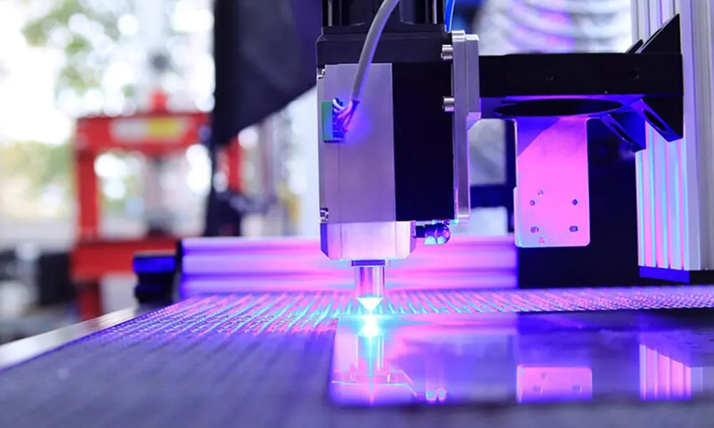
Turn operating conditions into build requirements
Start with where the board works, how it is loaded and how a failure affects the equipment. Use that information to agree the material, construction and verification plan with the responsible engineers.
| Operating condition | Question to resolve | Requirement to document |
|---|---|---|
| Heat and electrical load | What temperatures and loads occur at the board and components? | Material selection, copper/thermal design and test conditions |
| Vibration or mechanical stress | How are the board, connectors and heavy parts supported? | Mounting, component support and any mechanical qualification |
| Humidity or contamination | What exposure occurs inside the actual enclosure? | Cleanliness requirements and any protective treatment/qualification |
| Maintenance and service life | Which parts must remain replaceable or available? | Approved components, substitutions and change notification |
This table is a planning aid, not a universal industrial specification. A protected control cabinet and an exposed sensor installation should not inherit the same requirements without review.
Keep material selection separate from system qualification. NCAB’s material-selection guidance explains that materials with the same glass transition temperature (Tg) can have different thermal expansion characteristics. Tg alone is therefore insufficient for material selection, and one laminate property cannot describe the reliability of a complete assembly. If a higher-temperature material, protective coating or environmental test is proposed, ask which requirement it addresses and how its suitability will be checked. Avoid adding treatments solely because the application is called industrial.
The PCB manufacturing process, from files to bare boards
Bare-board fabrication forms the copper connections and insulating structure that assembly will use. The sequence below describes a typical multilayer subtractive process, consistent with NCAB’s multilayer production description. Special constructions, including sequential buildup and filled-via designs, can require additional operations and different routing through the factory.
1. Release the design and agree the route
The manufacturer reviews the released manufacturing data and checks whether the design can be made with the proposed process. Design for manufacturability (DFM) review addresses features such as spacing, holes and panel constraints. Stackup, material, copper, finish and outline requirements must agree across the released documents.
Checkpoint: unresolved engineering questions have a documented answer before affected production starts. A proposed change to a hole, material or stackup needs approval; a successful file import alone is not approval of that change.
2. Form and inspect the inner circuits
Copper-clad inner-layer material is imaged with the circuit pattern. In a typical subtractive route, unwanted copper is etched away and the remaining conductors form the circuits. Inner-layer inspection checks the pattern before the layers are bonded into the board.
Checkpoint: confirm the required inner-layer checks occur while the circuits remain accessible. Ask what inspection evidence accompanies the order if you need more than the supplier’s routine internal record.
3. Laminate, drill and connect the layers
The inner layers are aligned with insulating bonding material and copper layers, then pressed into a multilayer structure. Drilling makes the specified holes. Hole preparation and conductive deposition/plating create the connections required between layers; outer-layer processing forms the external circuits.
These operations are related but distinct. Drilling defines a hole’s geometry; metallization provides a conductive connection. Fine-feature and microvia constructions can change the equipment and sequence, so the agreed construction governs the route.
Checkpoint: match the approved stackup and hole requirements to the actual build. Where special inspection or verification is needed, include it in the order scope rather than assuming it follows from a layer count.
4. Apply mask and finish, then complete board verification
Solder mask protects selected areas while leaving the required pads exposed. Surface finish prepares exposed connection areas for subsequent use and soldering. Marking, profiling and electrical test complete the specified bare-board route; the order of some finishing, profiling and test operations can vary.
Bare-board electrical testing checks the intended connections for faults such as opens and shorts. It does not demonstrate that the future populated circuit will operate correctly.
Checkpoint: confirm the released revision, outline, panel delivery format and agreed test result. If boards must arrive in assembly panels, include that requirement before profiling is finalized.
Altium’s manufacturing-process guide, updated September 8, 2025, separates bare-board fabrication from assembly and describes the imaging, etching, lamination, drilling and plating route. Check the selected supplier’s actual sequence against the order’s agreed technical requirements.
Assemble components and approve the first build
Assembly adds a second set of inputs and failure risks: components, placement data, soldering and any programming or functional checks. Keep the assembly revision aligned with the approved bare board.
Prepare parts and run the assembly route
Agree the bill of materials (BOM), component placement list (CPL), assembly drawing and approved substitutions. Incoming checks should follow the agreed sourcing and quality plan.
For surface-mount technology (SMT), the typical route is solder-paste printing, component placement and reflow soldering. Solder paste inspection (SPI), when specified, checks the paste deposit before later operations. Eurocircuits’ solder-paste printing guidance describes inspection of deposit volume, offset and height before placement. Through-hole components may use selective, wave or hand soldering according to the assembly and process. Mixed assemblies can need several passes.
Avoid treating one oven setting or soldering route as suitable for every build. The components, solder material and board construction determine the process requirements.
Compare the first build with the approved requirements
First-article review checks whether the initial build matches the approved assembly information. Confirm component identity and orientation, mechanical fit, programming revision where applicable, and required inspection/test results. Agree the sample quantity and approval scope in advance.
An unresolved first-article issue needs a disposition: correct it, obtain an authorized concession, or hold the affected work. Record which decision applies to subsequent units. Pilot approval should identify what was accepted, rather than rely on a photograph of a populated board.
PCB quality control: match each check to a failure risk
A useful inspection plan explains what each check covers and which evidence supports acceptance. Choose the methods around the design’s risks and the agreed specification; do not treat a list of machines as a complete test plan.
What each inspection or test can establish
The table below is a suggested buyer checklist. Its evidence column lists records to request and agree, not documents every supplier automatically includes.
| Stage and risk | Check to agree | Preuves à demander | Limit to recognize |
|---|---|---|---|
| Inner circuits: pattern defects before bonding | Inner-layer inspection | Lot/revision identification and inspection disposition | Does not establish finished-board connectivity |
| Bare board: open or short circuits | Electrical test against approved connectivity | Test scope, lot identification and result | Does not establish assembled circuit function |
| Paste printing: missing, excessive or misplaced paste | SPI where specified | Inspection result and exception disposition | Checks the deposit before soldering |
| Populated board: visible placement or solder defects | Automated optical inspection (AOI) and visual checks | Inspection scope and resolved exceptions | Hidden connections can remain outside optical coverage |
| Hidden joints: features obscured beneath packages | X-ray where specified | Images/results assessed against agreed criteria | Does not prove circuit operation |
| Completed assembly: incorrect behavior | Defined power-on/functional test | Procedure revision, conditions and results | Coverage is limited to the functions and conditions tested |
European Circuits’ test overview distinguishes bare-board open/short testing from assembly inspection and customer-defined functional testing. Eurocircuits’ X-ray explanation describes inspection of concealed package connections. These sources describe different checks, not interchangeable proof of a complete assembly’s performance.
Use the supplier’s inspection and testing capabilities to discuss which methods are available for the proposed build. Functional testing requires agreed procedures and, where needed, fixtures, firmware and test interfaces.
Agree acceptance standards and qualification scope
The standards must match the deliverable. IPC’s Meet Your Standards overview describes these distinct document subjects:
- IPC-6012 : qualification and performance specification for rigid printed boards.
- IPC-A-600 : acceptability of printed boards.
- IPC-A-610: acceptability of electronic assemblies.
- J-STD-001: requirements for soldered electrical and electronic assemblies.
Agree the applicable documents, revisions, class and any product-specific requirements. Standard titles alone do not supply acceptance limits or prove supplier certification.
Routine production checks also need a separate scope from environmental or life qualification. A functional pass at the agreed bench conditions cannot establish performance across untested temperatures, vibration or lifetime exposure. If qualification or burn-in is needed, define its conditions, duration, sample plan and responsibility explicitly. Confirm availability rather than assuming these services are included.
What changes production cost and lead time?
PCB production cost and lead time depend on the approved construction, parts and verification work. Compare quotations against the same scope before comparing unit prices or delivery dates.
| Driver | What to clarify before accepting a quote |
|---|---|
| Material and stackup | Approved grades, availability and permitted alternatives |
| Copper, holes and special structures | Required process route and any additional operations |
| Panel layout and quantity | Delivery format, tooling and what changes between prototype and repeat order |
| Components | Availability, purchasing responsibility and substitution approval |
| Test development | Required fixture, procedure, firmware and engineering effort |
| Open questions | Which approvals or missing inputs prevent the schedule from starting |
Separate quotation time, component procurement, engineering approval, manufacturing and shipping. A manufacturing lead time does not necessarily include all five. Ask the supplier to state the start condition and what happens if an approval or component is delayed.
A lower assembly price may also cover fewer tests or exclude fixture development. Identify those differences explicitly. Compare the delivered item, acceptance scope and required records alongside the quoted price.
Approve repeat production with a clear release record
A repeat order needs an identifiable approved baseline. Link the fabrication and assembly revisions to the agreed parts, inspections and test procedure, then record any exceptions before release.
Illustrative example: the control-board record below is fictional and demonstrates the fields to agree. It is not a customer case or evidence of completed production.
| Release field | Illustrative entry |
|---|---|
| Bare board | Control board, fabrication revision C |
| Assembly baseline | Assembly drawing C2, BOM C2 and placement data C2 |
| Component substitution | Alternate input connector proposed; approval pending |
| Agreed checks | Bare-board electrical test, assembly inspection and functional test under procedure FT-C2 |
| Test evidence | Pilot results available; repeat-build acceptance must use the released procedure |
| Open deviation | Alternate connector has not been approved for fit and electrical suitability |
| Release decision | Hold work affected by the substitution until approval or use the approved part |
| Release authority | Named customer approver and supplier contact recorded in the actual job record |
The hold is specific: a proposed substitute is not part of the approved baseline until the responsible party accepts it. Inspection results from a different configuration do not automatically clear that change.
After disposition, update the release record so the next order identifies the accepted configuration. For the wider pre-award audit and supplier controls, use the liste de contrôle de qualification des fournisseurs PCB.
Frequently asked questions
What is the difference between PCB fabrication and PCB assembly?
Fabrication produces the bare board, including its copper circuits, insulating layers, holes, mask and finish. Assembly mounts and solders components onto that board. Programming, functional testing and integration are additional scope items to agree. Request a quote that states which deliverable and acceptance checks are included.
Does every industrial PCB require Class 3?
Specify the applicable acceptance class from the product’s requirements and the agreed standard. The word industrial does not define that contract. Ask the responsible engineering and quality parties to select the applicable requirements and confirm the supplier can meet them. Do not substitute a general marketing claim for the order specification.
Does AOI replace electrical or functional testing?
AOI examines visible features for the defects covered by its inspection setup. Bare-board electrical testing checks connectivity, while functional testing checks defined circuit behavior. Their purposes differ. Agree a combined plan that covers the relevant risks and states the remaining limits, especially for hidden connections and untested functions.
Does every industrial assembly need X-ray or burn-in?
The need follows the package construction, failure risks and customer requirements. X-ray can support assessment of hidden joints; burn-in requires its own defined conditions and acceptance plan. Neither should be assumed to be part of every assembly order. Confirm the method, scope, availability and evidence before accepting the quote.
What should be agreed before repeat production?
Identify approved fabrication and assembly revisions, parts and substitutions, inspection/test scope, required records, open deviations and release authority. State how subsequent changes require approval. A repeat part number alone does not identify every manufacturing input or prove that the same verification scope will be used.
Plan your industrial PCB build
Submit your released design package, operating requirements and requested verification scope for an industrial PCB assembly review. Ask for confirmation of the construction, assembly route, test coverage and schedule start conditions before authorizing production.