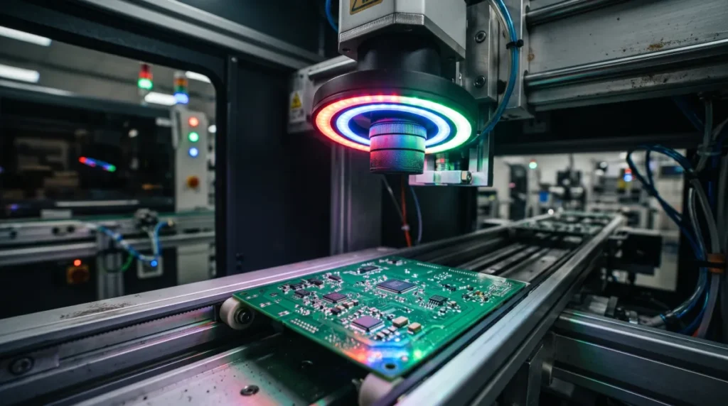
What is AOI? Automated optical inspection uses cameras, lighting and software to check a circuit board for specified visible features or possible defects. In PCB assembly, it can flag missing components or exposed solder bridges. AOI can also check bare-board copper patterns, but it cannot see every hidden joint or confirm that a board works.
For an assembly buyer, the useful question is not just whether a supplier offers AOI. It is what the cameras can see, what the inspection program checks and how the team handles a flagged result.
Key Takeaways
- AOI can identify programmed, visible conditions such as missing parts, misplaced components and some exposed solder bridges.
- Detection depends on the camera view, lighting, inspection program and acceptance criteria. A pass does not establish that every possible defect is absent.
- SPI, X-ray, in-circuit testing and functional testing answer different questions and may be specified alongside AOI.
- Before ordering, agree on the inspection stage, coverage, review process and records available for the build.
How automated optical inspection works
AOI captures images of a board and checks selected features against a programmed reference. A system typically aligns the board to known reference points, illuminates it, records one or more views and evaluates those images using inspection rules or comparison data. It then flags features that fall outside the configured limits for review.
The program can use placement data, component libraries, reference images and other design information. The inputs vary by machine and setup. A camera cannot recognize a part value or polarity simply because that information appears in the bill of materials: the relevant distinguishing feature must be visible and the check must be configured to use it.
An operator or quality team can review flagged images against the project’s acceptance criteria. A flag is an indication to investigate, not automatically a confirmed defect. The response may include accepting the feature, repairing the board or checking it again, according to the agreed process.
Bare-board inspection and assembly inspection
AOI is used at different points in manufacturing. During bare-board fabrication, it can compare exposed copper patterns with reference information to identify potential pattern defects. The HDI manufacturing process describes inspecting inner layers before later lamination.
During assembly, AOI instead checks features such as component position and exposed solder connections. The rest of this guide focuses on assembly AOI, where the board’s packages, markings and solder joints determine what an optical system can inspect.
Where AOI fits in PCB assembly
Assembly AOI can be placed after components are positioned, after reflow soldering, or at both stages when the line and project call for it. The inspection point affects which conditions can be examined.
A typical surface-mount sequence is:
- Print solder paste. Paste is deposited through a stencil onto the board’s pads.
- Inspect paste when specified. Solder paste inspection, or SPI, checks deposits before components cover them.
- Place components. The placement machine positions parts on the paste.
- Inspect before reflow when specified. AOI may flag visible placement or orientation issues before soldering.
- Reflow and inspect again when specified. After solder melts and solidifies, AOI can check accessible component features and exposed joints.
- Review results and perform other agreed checks. The plan may include X-ray or electrical tests where needed.
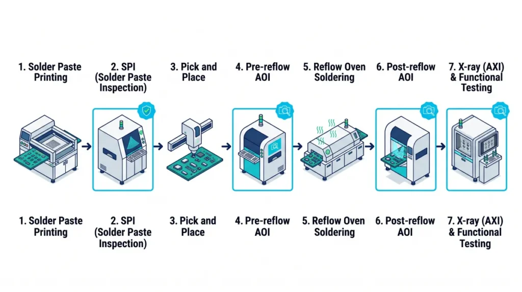
This is a possible sequence, not a claim that every order uses every station. FLJ PCB’s inspection overview describes SPI after paste printing and AOI after reflow as complementary checks. The solder paste inspection guide explains paste measurements in more detail, while the reflow soldering guide covers the heating process.
What defects can AOI detect?
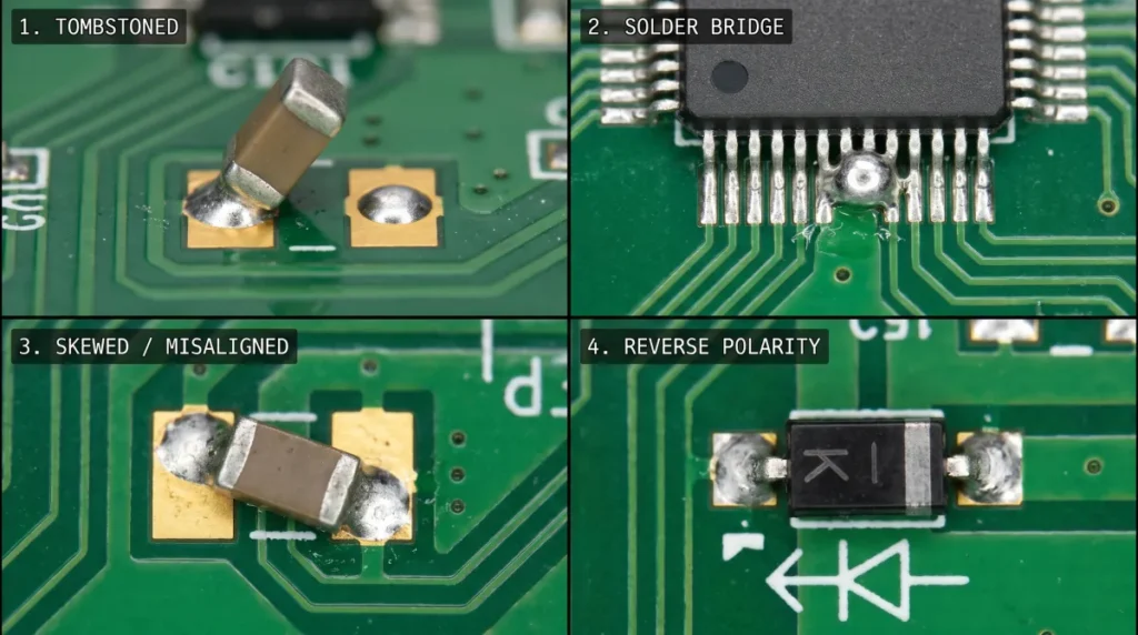
AOI can flag visible assembly conditions when the system has a suitable view and a programmed check for the feature. Koh Young’s inspection overview lists examples including missing or misplaced parts, tombstoning and exposed solder bridges. Actual coverage must be established for the board being built.
| Condition | What AOI may check | Important limit |
|---|---|---|
| Missing component | Whether an expected part is present at its location | The program needs the correct location and reference for that part. |
| Misaligned component | Position or angle relative to its expected footprint | Nearby parts, glare or limited camera angles can obscure a feature. |
| Tombstoned component | A small part lifted at one end | Detection depends on the view and system capability. |
| Incorrect orientation or polarity | A visible mark or feature compared with the required orientation | An obscured or indistinguishable mark cannot establish polarity by itself. |
| Exposed solder concern | Visible bridges or an apparent shortage of solder at an accessible joint | A surface image does not reveal every hidden joint or prove its integrity. |
AOI may also flag a wrong component when a visible marking, shape or other programmed feature differs from the reference. Two electrically different parts that look the same to the camera require another way to establish identity. Conversely, a substitute component with a different appearance may trigger a flag even when it is approved for the build.
AOI limitations: what inspection cannot see or prove
AOI is a line-of-sight inspection method. A camera view of the top and sides of a package does not expose every connection underneath it. For example, many ball grid array (BGA) solder joints are concealed by the component body. Koh Young’s AOI overview describes these hidden joints as a limit of optical inspection.
A board can also have a fault that looks normal from the outside. An internal break, an incorrect value on an indistinguishable component or a firmware problem needs evidence beyond a surface image. Binghamton University’s X-ray facility lists semi-automatic BGA solder-joint inspection, an example of how X-ray can help examine concealed features. Electrical and functional tests answer different questions when they are appropriate for the build.
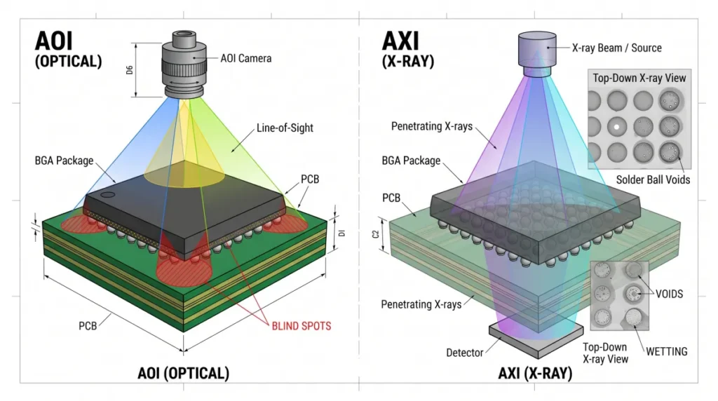
An AOI pass means the configured inspection did not leave a reported failure under the applicable process. It is not a guarantee of full defect coverage, electrical performance or compliance with every requirement in an assembly standard. The relevant criteria come from the drawings, customer requirements and any standard agreed for the order.
2D vs 3D AOI: what changes?
A 2D AOI system evaluates features in images, which may come from more than one viewing angle. A 3D system can add surface-height information to images, giving the inspection program another way to assess geometry. Neither label alone tells a buyer exactly what a particular board inspection will cover.
| Inspection approach | Information used | Practical consideration |
|---|---|---|
| 2D AOI | Image features such as position, shape and visible markings | Useful for features the camera can distinguish in the available view. |
| 3D AOI | Image features plus height information, depending on the system | Height can help assess features such as raised leads, subject to access and setup. |
Koh Young’s explanation describes 3D AOI as reconstructing surface height across the field of view. That added information does not make a hidden BGA joint optically visible, and it is not a promise that every defect will be detected. Ask which features and inspection points are included for the actual assembly.
AOI vs SPI, X-ray and electrical testing
These methods provide different evidence. Choosing one starts with the question the inspection or test needs to answer.
| Method | What it can help assess | Example limitation |
|---|---|---|
| SPI | Paste deposit features after printing, before placement | It does not establish the quality of a finished reflowed joint. |
| AOI | Programmed, visible component and solder features | It cannot inspect every obscured or internal feature. |
| X-ray | Some concealed joints and internal solder features | An image alone does not prove that firmware or the complete product works. |
| In-circuit or functional testing | Selected electrical connections, component behavior or product functions | Coverage depends on the chosen method, access, fixtures and test procedure. |
For example, in-circuit testing may check selected electrical connections or components, while a functional test exercises specified behavior. Micron’s comparison of inspection and test methods notes that in-circuit coverage depends on probe access, fixture design and test planning. Neither a test name nor a supplier’s general capability list defines the coverage of a particular order.
A NASA evaluation of solder-joint inspection compared optical and X-ray techniques for low-volume, high-reliability surface-mount assemblies in 1993. Its results describe the systems tested, not a detection guarantee for today’s machines.
How an AOI program and its findings are reviewed
A useful inspection plan connects the board revision, the features to be checked and the criteria for deciding what happens next. Ask the assembler how the program will be prepared and validated for the build.
Set up and validate the checks
Provide the current assembly drawing, bill of materials and placement information needed for review. Agree on the relevant board and component revisions, inspection point, orientation references and criteria for visible features. A known-good reference can help setup, but one good board alone does not demonstrate that the program will recognize every defect of interest.
Ask which features the system can inspect and where package geometry, markings or access create exclusions. The IPC-A-610 assembly acceptance guide explains the broader acceptance framework; the edition, class and customer requirements for a specific order must be agreed separately.
Review false calls and possible escapes
A false call is a flagged feature that review finds acceptable under the applicable criteria. A defect escape is a real defect that reaches a later stage without being caught by the intended check. These are different problems: adjusting a program to reduce nuisance flags must not remove useful coverage.
A 2024 research dataset described by the University of Helsinki includes AOI flags assessed in manual inspection as true defects or false calls. That record of reviewed flags illustrates how teams can study false calls; it does not by itself establish how many defects passed AOI unnoticed.
Agree on who reviews flagged images, how a confirmed defect is handled, and whether repaired boards are reinspected. To evaluate missed defects, a supplier needs an independent way to establish what was actually present, such as an agreed validation set or supplementary inspection. AOI pass records alone cannot reveal every missed defect.
Worked example: one board, four inspection questions
Consider a hypothetical assembly with an exposed fine-pitch lead, a diode with a visible polarity mark, an unmarked component that looks identical to the wrong part, and a BGA whose central joints are hidden underneath. The table illustrates questions for the inspection plan; it is not a record from a real production run.
| Question on the board | What AOI may establish | Follow-up to agree |
|---|---|---|
| Is there an exposed bridge between the fine-pitch leads? | It may flag a bridge if the area is visible and the check is configured. | Confirm camera access, acceptance criteria and how a flag is reviewed. |
| Is the marked diode oriented correctly? | It may compare the visible mark and position with the programmed reference. | Confirm the polarity reference in the drawing and that the mark can be seen. |
| Is the unmarked, look-alike component the correct value? | Its appearance alone cannot distinguish it from an identical-looking wrong part. | Agree on component identification, traceability or a suitable electrical check. |
| Are the concealed central BGA joints acceptable? | A top-view image cannot directly show joints hidden under the package. | Determine whether X-ray and any electrical checks are needed for the project. |
The outcome is an agreed scope, not simply “AOI required.” For the quote, request the inspection stage, features or exclusions, governing criteria, review and reinspection process, and any results or records the supplier can provide. Discuss hidden-joint and electrical test needs separately.
Frequently asked questions
Is AOI the same as visual inspection?
AOI automates image capture and programmed checks. Human visual inspection relies on a person examining the board, sometimes with magnification. The two can work together: a person may review an AOI flag against the applicable criteria or examine features outside the automated program’s scope.
Can AOI inspect BGA solder joints?
AOI can check visible external features of a BGA assembly, but it cannot directly inspect joints hidden beneath the package body. X-ray may be used to examine concealed solder features when the project requires it. The exact inspection and acceptance plan should be agreed before production.
Does an AOI pass guarantee that a board works?
No. An AOI pass covers the configured optical checks under the inspection conditions. It does not demonstrate every electrical connection, component function or firmware behavior. Specify electrical or functional testing separately when those results are needed.
Specify inspection before requesting a quote
Start with the board revision, drawings, bill of materials and the features that matter most to the product. Then ask the PCB assembly team which AOI checks, hidden-joint inspections and test records can be agreed for that build. Clear scope makes a pass or a flagged result more useful when the board reaches review.