A rigid-flex PCB combines rigid circuit regions and flexible circuit layers in one construction. The rigid regions support components and can contain additional conductive layers, while the flexible region connects them through the enclosure. Conductors cross each rigid-to-flex transition to carry signals and power between regions.
다음과 같은 hypothetical compact device with a populated control region and a populated interface region on different sides of an internal enclosure corner. A flexible connection must route around that corner. For this example, the flex is bent during installation and remains stationary during normal operation; service handling still needs consideration. A rigid-flex design is one option alongside separate rigid boards with a cable and a flex circuit with local stiffeners.
핵심 요점
- Compare packaging, connections, assembly, service and validation before choosing rigid-flex over a cable or stiffened flex.
- Define the rigid and flex stackups together. A passive stiffener supports a flex circuit but does not add integrated rigid circuit layers.
- Route conductors through transitions, while placing the actual bend and stress-sensitive features away from those interfaces using fabricator-approved clearances.
- Specify how the assembly bends and is handled. Repeated movement calls for qualification under representative conditions, with agreed electrical pass/fail criteria.
- Compare the complete assembly cost and send the fabricator the regional construction, mechanical constraints and test requirements for a useful quote.
When does a rigid-flex PCB make sense?
Rigid-flex is worth evaluating when connecting populated regions inside an enclosure creates a difficult packaging or assembly problem. For the hypothetical device, each of the three architectures changes where connections, assembly work and validation occur.
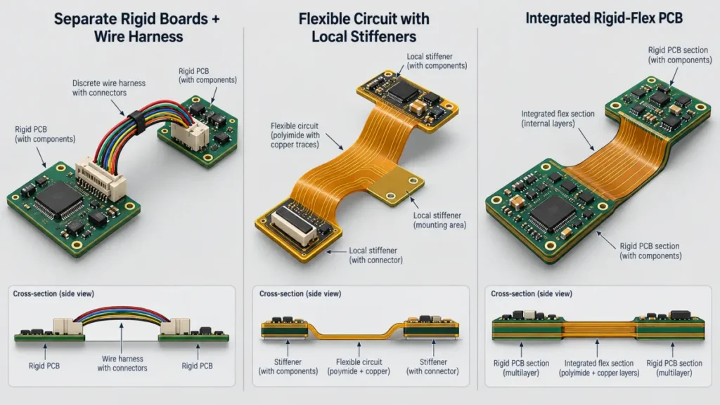
| Architecture | Packaging and connections | Service and verification |
|---|---|---|
| Rigid boards and cable | Boards link by cable; connectors need mating space. | Boards may be replaceable separately; check the cable path and contacts. |
| Stiffened flex | Continuous flex links supported component areas. | The circuit may need replacement as a unit; check joints and flex. |
| 리지드-플렉스 | Flex links rigid circuit regions; it can remove their cable and connectors. | The assembly may need replacement as a unit; check transitions and connections. |
Separate rigid boards can be designed independently, but the cable must be routed and mated during assembly. Replacing a board separately depends on connector access. Check connector retention and service access as well as the cable path and electrical contacts. The guide to rigid PCB construction covers the board side of this option.
Stiffened flex can connect locally supported component areas without an internal board-to-board cable. Passive stiffeners do not add electrically integrated rigid-board copper layers. Component assembly can require support fixtures; check enclosure fit, supported-area assembly, solder joints and flex behavior.
Rigid-flex integrates flexible circuitry with rigid regions that have their own conductive layers. The single assembly needs a coordinated stackup and manufacturing process. Check interlayer connections, transitions, mechanical fit and assembly access.
None of these choices wins for every device. A removable cable may be valuable for repair; integrated rigid-flex may be useful when the cable and mating space are difficult to accommodate. Cusack Electronics’ rigid-flex guide discusses construction and the distinction from stiffened flex. The broader guide to flex PCB types and design choices covers other flex configurations.
For the rest of the example, assume the team selects rigid-flex because the enclosure makes the internal cable and connectors awkward. That is a design hypothesis to check with a mechanical model, prototypes and supplier quotes, not a demonstrated saving.
How is a rigid-flex PCB stackup built?
A rigid-flex stackup defines which materials and conductive layers exist in each region and how they connect. A design might use a polyimide-based flexible circuit with copper conductors that continues into both rigid areas. The rigid areas can add glass-reinforced epoxy material such as FR-4 and further copper layers; plated connections in the rigid regions can connect those layers to the flex circuitry.
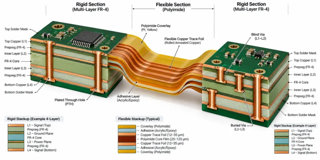
The exposed flexible span needs its own defined construction. A coverlay can protect copper on a flex surface, with openings where the design needs access; adhesives or bonding layers may also be part of the build. Layer order, materials and bonding choices depend on the design and fabricator. A rigid-to-flex transition is the interface where the rigid construction ends and the flexible span continues.
For the device, propose the flexible conductors needed between control and interface regions, identify the extra copper needed within each rigid region, and show where the relevant connections change layers. Ask the fabricator to review the complete regional stackup before treating it as buildable.
Design the transition and flexible region
Route through the rigid-to-flex transition
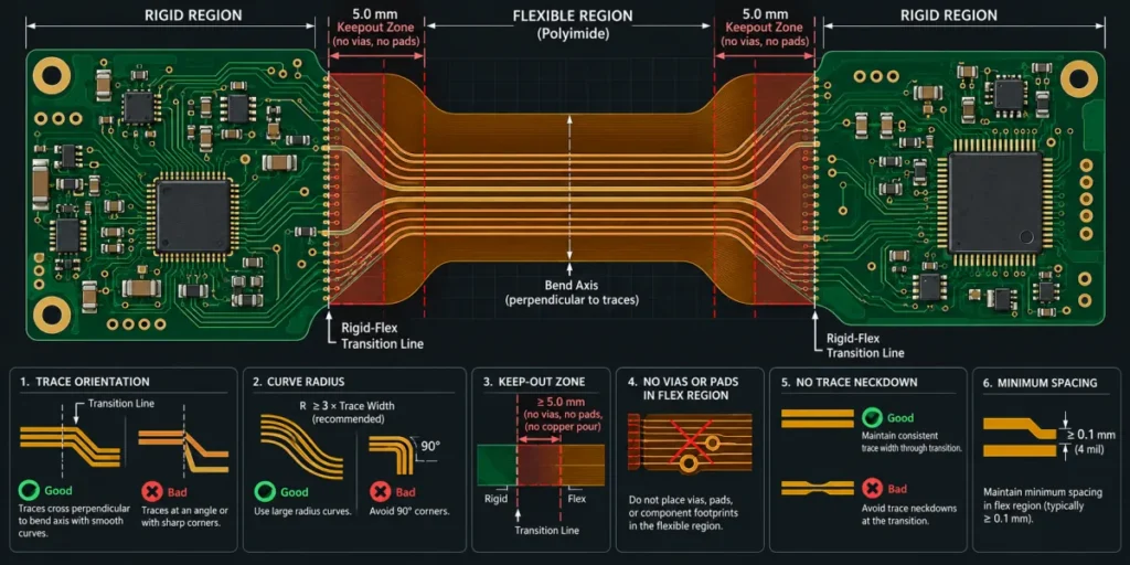
Traces must cross the transition to connect the rigid and flexible regions. Route them smoothly through the interface and avoid abrupt direction or width changes there. Where appropriate, route conductors across a bend approximately perpendicular to its axis; check the actual bend geometry and electrical routing needs before fixing the orientation.
Place pads, vias, plated holes and abrupt neckdowns away from transitions and active bend areas using clearances approved for the proposed construction. All Flex’s rigid-flex guidance recommends waiting until traces have exited the rigid area and cleared the keepout margin before necking them down, and advises against placing vias close to the boundary. Put the intended bend within the flexible span, away from the rigid interfaces, subject to the fabricator’s review. The clearance depends on the stackup and use, so a generic fixed keepout is not a substitute for an agreed drawing.
In the hypothetical enclosure, the conductors leave the control region, continue through the flex around the corner and enter the interface region. Show both transition boundaries and the intended bend on the drawing. Check that the available straight portions and enclosure clearance allow the bend to occur where planned, without pinching the flex or placing it against a sharp feature.
Define the bend and the motion
Mark the bend axis, the line about which the flex curves, as well as the bend location, direction and installed geometry. Check the design in three dimensions with the enclosure and assembly sequence. Include expected tolerances, any contact with the housing, and the path the flex takes while the product is opened or serviced.
이 예제는 정상 작동 중에는 구부러진 상태를 유지하도록 설계되었습니다. 이는 사용 중 반복적으로 움직이는 플렉스와는 다르지만, 설치와 수리 과정에서도 움직임이 발생할 수 있습니다. 실제 움직임을 고려해 구리 종류, 층 구조, 장착 상태와 그에 따른 변형을 모두 검토해야 합니다. Sierra Circuits의 플렉스 설계 지침 에서는 배선 및 굽힘 관련 고려 사항을 다룹니다. 굽힘 계산과 수치 예시는 별도의 플렉스 PCB 굽힘 반경 가이드.
재료와 영역별 적층 구조 지정
표준 경성 기판 적층 구조가 조립체 전체에 적합할 것이라고 가정하지 말고, 제조업체가 전기적 및 기계적 요구 사항을 모두 검토할 수 있도록 충분한 정보를 제공하세요.
- 층 구성: 각 경성 영역과 플렉스에 포함되는 층, 층의 순서, 사용 예정 재료, 구리 사양, 커버레이, 개구부 및 접착층을 명시하세요. 영역의 경계와 제안하는 층간 연결 방식도 정의하세요.
- 구리와 움직임: 의도된 굽힘을 설명하고, 해당 용도에 적합한 구리 종류, 두께, 가공 방식 및 방향을 제조업체가 검토하도록 요청하세요. 적절한 선택은 완성된 구조와 움직임 모두에 따라 달라집니다.
- 전기적 동작: 전환부를 지나는 신호 경로와 귀환 경로를 표시하세요. 필요한 경우 해당 영역에 대한 임피던스, 간격 및 전기적 성능 목표를 지정하고, 적층 구조의 변화가 어떻게 평가될지 문의하세요.
- 환경 및 조립: 장치가 견뎌야 하는 온도, 습기, 화학 물질 또는 기타 조건과 관련 조립 및 서비스 제약 사항을 명시하세요. 재료 선택에 관한 내용은 PCB 재료 가이드.
예제에서 제안된 플렉스는 필요한 제어부와 인터페이스 간 연결을 유지하면서 모서리에 맞아야 합니다. 필요한 배선 때문에 플렉스 구조가 달라진다면, 설계를 확정하기 전에 기계적 장착 상태와 전기적 성능을 모두 다시 검토하세요.
제조 및 조립이 설계에 미치는 영향
리지드-플렉스 제조에서는 경성 영역과 유연 영역이 의도한 대로 정렬되고 접합되어야 합니다. All Flex의 제조 개요 에서는 순차 적층, 정렬, 수지 흐름 및 커버레이를 다룹니다. 실제 공정 순서는 제안된 구조에 따라 달라지므로, 초기에 제조업체와 함께 적층 구조와 도면을 검토하세요.
공급업체가 플렉스 영역을 어떻게 성형하고 보호할지, 정렬을 유지하고 경성부와 플렉스부의 접합부를 검사할지 문의하세요. 패널화, 툴링, 제조 및 조립 과정에서 회로를 취급하는 데 필요한 지지 방안도 논의하세요. 부품을 배치하고 납땜하는 동안 조립체를 지지하기 위해 캐리어나 고정구가 필요할 수 있습니다.
소형 장치에서는 두 경성 영역 모두에서 부품, 검사 지점 및 필요한 경우 재작업 부위에 접근할 수 있는지 확인하세요. 또한 작업자가 플렉스를 하우징에 억지로 밀착시키지 않고 회로를 설치할 수 있는지도 확인하세요. 접은 뒤 어느 한 영역을 검사하거나 수리하기 어렵다면, 이는 조립 계획뿐 아니라 아키텍처 선택에도 영향을 줄 수 있습니다.
리지드-플렉스 PCB 비용에 영향을 미치는 요인은 무엇인가요?
리지드-플렉스 비용은 구조와 제조 및 검증에 필요한 작업에 따라 달라집니다. 영역별 층수, 재료 선택, 적층, 정렬, 컷아웃, 패널 활용률, 수율, 검사 및 주문 수량이 모두 견적에 영향을 줄 수 있습니다. 복잡한 단일 부품은 어느 한 영역에 결함이 생겼을 때 폐기 또는 교체 비용에도 영향을 미칠 수 있습니다.
가상의 장치에 대해서는 세 가지 아키텍처 모두를 다음과 같은 동일한 항목으로 비교하세요:
- 무장착 회로 및 상호 연결 부품: 각 설계에 실제로 필요한 케이블과 커넥터를 포함해, 별도 기판, 보강된 플렉스 또는 리지드-플렉스 조립체의 제조 비용을 비교하세요.
- 조립 및 시험: 해당하는 경우 커넥터 결합, 고정구, 취급, 검사 및 전기적 또는 기계적 적격성 평가를 포함하세요.
- 서비스: 접근성을 고려하고, 고장 난 영역만 별도로 교체할 수 있는지 아니면 더 큰 조립체 전체를 교체해야 하는지 검토하세요.
내부 케이블과 커넥터를 제거하면 견적 대상 부품과 작업이 달라질 뿐, 리지드-플렉스의 총 조립 비용이 가장 낮다는 뜻은 아닙니다. 동일한 수량, 합격 기준 및 서비스 가정을 적용해 비교 가능한 견적을 요청하세요.
양산 전에 설계 시험하기
전기 시험, 기계적 장착 확인 및 플렉스 적격성 평가는 각각 서로 다른 질문에 답합니다. 결과를 근거로 설계를 확정하기 전에 시료, 방법 및 합격 기준에 합의하세요.
- 전기적 연결 및 절연: 시험할 네트와 연속성 및 절연에 대한 합격 기준을 정의하세요. 경성 영역 간 연결과 플렉스를 가로지르는 도체를 포함하세요.
- 구조 및 전환부 검사: 영역 경계, 커버레이 및 관련 제조 특성을 어떻게 검사할지 합의하세요. 제작 구조에 필요한 추가 검사나 대표 단면 분석도 지정하세요.
- 장착 및 취급: 대표 조립체를 하우징에 설치하세요. 장치에서 예상되는 굽힘 위치, 접촉 지점, 부품 접근성, 조립 및 서비스 동작을 확인하세요.
- 반복 굽힘(해당하는 경우): 실제 작동 중 발생하는 움직임을 정의하고 대표 회로나 맞춤형 시험 쿠폰의 적격성을 평가하세요. 굽힘 형상, 방향, 움직임 속도, 예상 수명을 기준으로 한 사이클 목표, 환경, 시료 계획 및 전기적 합격/불합격 한계에 합의하세요. 여기에는 전기 측정 시점도 포함해야 합니다. 시험 대상 특성을 구조와 배선에 반영해 시험 시편이 이를 대표하도록 하세요. 필요한 경우 조립된 제품도 별도로 확인하세요.
이 예제에서는 플렉스를 움직이지 않는 상태로 사용하는 것이 목적이므로 장착 및 취급 확인이 필요합니다. 이후 개정 설계에서 플렉스를 움직이는 힌지에 배치한다면, 해당 움직임을 반영한 대표 동적 시험을 추가하세요. 2025년 10월에 열린 PCEA Flexperts의 플렉스 시험 논의 에서는 플렉스 수명 적격성 평가가 거의 항상 맞춤형 시험이며, 사이클 횟수는 제품 수명 동안 예상되는 굽힘 횟수보다 많아야 한다고 설명합니다. 특정 시점에 연속성 시험을 통과했다고 해서 굽힘 수명이 입증되는 것은 아닙니다. 쿠폰 시험 결과는 완성된 설계 및 사용 조건을 얼마나 잘 대표하는지 고려해 해석해야 합니다.
IPC는 IPC-6013F 적격성 평가 및 성능 표준 개정판을 발표했습니다. 적용할 표준과 판, 등급 및 프로젝트별 합격 기준에 대해 제조업체와 합의하세요. IPC 규격 준수 선언만으로는 회로가 장치의 특정 움직임을 의도된 수명 동안 견딘다는 사실이 입증되지 않습니다. 플렉스 수명은 해당 용도에 맞게 적격성을 평가해야 합니다.
리지드-플렉스 PCB 제조업체에 무엇을 보내야 하나요?
조립체의 평면 상태와 설치 상태를 모두 설명하는 제조 패키지를 보내세요. 가상의 장치에서는 제어부와 인터페이스 영역을 표시하고, 두 영역 사이를 플렉스가 어떻게 연결하는지 보여주세요. 다음 내용을 포함하세요:
- 보드 외곽선, 레이어 매핑, 드릴 데이터, 영역 경계, 관련 치수 및 공차가 포함된 제조 파일과 도면.
- 제안된 리지드 및 플렉스 적층 구조, 구리 및 재료 요구사항, 커버레이 개구부, 표면 마감, 의도된 층간 연결.
- 굽힘 축, 방향, 위치 및 필요한 설치 형상. 설치 중, 사용 중 또는 반복 작동 중에 움직임이 발생하는지 명시하세요.
- 간격, 부품 접근성 및 유용한 기계 모델을 포함한 인클로저 및 조립 제약 조건. 조립이 범위에 포함된다면 조립 정보를 제공하세요.
- 작동 환경과 반복적으로 움직이는 경우의 동작, 목표 사이클 수 및 검증 조건.
- 시제품 및 양산 수량, 일정, 요청 표준 및 판본, 등급, 전기·검사·기계 시험의 합격 기준.
최종 승인 전에 제조업체에 제안된 구조, 제조 역량, 전환부 및 굽힘부의 간격, 시험 접근법과 가정 사항을 확인해 달라고 요청하세요. 견적에 의존하기 전에 평면 도면과 설치 모델 간의 차이를 해결하세요.
리지드-플렉스 PCB FAQ
보강 플렉스는 리지드-플렉스와 같은 것인가요?
아니요. 보강재는 플렉스 회로의 일부를 기계적으로 지지하지만, 그 자체로 전기적으로 통합된 리지드 PCB 레이어를 추가하지는 않습니다. 리지드-플렉스는 하나의 구조 안에 플렉스 회로와 리지드 회로 영역을 결합합니다. 두 방식은 비슷한 패키징 요구에 쓰일 수 있으므로 실제 장치의 부품 지지, 조립 및 서비스 요구사항을 기준으로 비교하세요.
리지드-플렉스 회로를 반복적으로 움직이도록 설계할 수 있나요?
네. 다만 적합성은 회로의 구조와 견뎌야 하는 움직임에 따라 달라집니다. 작동 형상과 환경을 지정한 다음, 대표성 있는 동적 시험, 목표 사이클 수 및 전기적 합격/불합격 기준에 합의하세요. 설치 후 굽혀진 상태를 유지하도록 설계된 회로와 사용 중 계속 움직이는 회로는 용도를 다르게 설명해야 합니다.
소형 장치 사례에서 다음으로 결정할 사항은 제안된 영역별 적층 구조와 설치 형상을 조립품의 제약 조건 내에서 제작하고 검증할 수 있는지 여부입니다. 이러한 요구사항이 준비되면 리지드-플렉스 PCB 제조 페이지 에서 제조 견적을 요청하세요.