Montagem de PCBs
Aqui, você pode adquirir conhecimento profissional abrangendo toda a cadeia, desde o projeto de PCBs até a montagem, além de uma análise precisa das tendências mais recentes da indústria eletrônica.
O que é a inspeção de pasta de solda (SPI)? Medições, defeitos e controle de qualidade
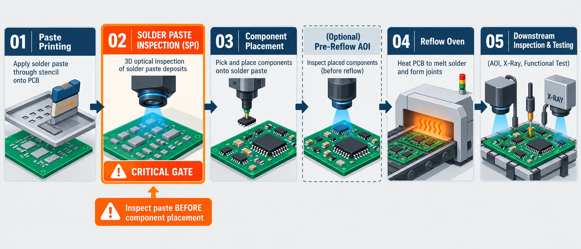
A inspeção de pasta de solda (SPI) verifica a pasta depositada em uma PCB após a impressão e antes da colocação dos componentes. Um sistema SPI 3D mede o volume, a altura, a área e o alinhamento do depósito em relação aos limites programados. Isso permite reter e corrigir impressões defeituosas antes da colocação e da refusão. Para engenheiros de hardware e compradores de PCBA, a principal decisão é saber se o…
O que são encapsulamentos QFN? Um guia prático para projeto e montagem de PCBs
Encapsulamentos QFN aparecem em tudo, desde fontes de alimentação e módulos sem fio até sensores, microcontroladores e sistemas eletrônicos automotivos. Seu pequeno footprint, os caminhos elétricos curtos e a transferência eficiente de calor fazem deles uma alternativa atraente aos encapsulamentos maiores com terminais. No entanto, as mesmas conexões inferiores que economizam espaço também tornam o projeto do footprint, a soldagem e a inspeção de QFNs menos tolerantes a erros. Portanto,…

BOM para montagem de PCBs: como preparar uma BOM de PCBA organizada
A BOM for PCB assembly is more than a spreadsheet of parts. It is the sourcing and assembly control document that tells a PCBA manufacturer what to buy, what to populate, what to leave off, and which substitutions are allowed. If the BOM is unclear, the RFQ stalls before production ever starts. Many PCBA RFQ…
Gerber, BOM, CPL e Stackup: o que cada arquivo significa
Gerber, BOM, CPL, and stackup files tell a PCB manufacturer four different things. Gerber files define the board layers. The BOM defines components. The CPL defines placement. The stackup defines layer construction, materials, copper, dielectric thickness, and impedance assumptions. Many PCBA quote delays happen before production starts. Why? The factory may have board data, but…

Quais arquivos são necessários para uma cotação de PCBA?
A PCBA quote needs more than Gerber files. For an accurate PCB assembly quotation, send Gerber files, drill files, BOM, CPL, stackup if needed, quantity, lead-time target, and test requirements. These files tell the manufacturer what to fabricate, what to source, where to place parts, and how the finished board should be accepted. If those…


Lista de verificação de DFM para PCB
A PCB DFM checklist helps engineers and buyers catch manufacturability problems before a board is quoted, fabricated, assembled, or released to production. The goal is to confirm that the supplier can build the design with the required stackup, tolerances, finish, test plan, and documentation. DFM review reduces engineering holds and helps buyers compare suppliers. If…
Guia de Vias de PCB: Tipos, Regras de Projeto e Dicas de Seleção
A PCB via is a plated interconnect that lets signals, power, ground, or heat move between copper layers in a printed circuit board. Via choice affects routing density, fabrication cost, assembly yield, signal integrity, and thermal performance, so it should be part of stackup and DFM planning, not a cleanup step at the end. For…

IPC-A-610: O guia completo para aceitação de conjuntos
IPC-A-610 is the acceptance standard that decides whether a finished printed circuit board assembly is good enough to ship. It is the document your contract manufacturer's inspectors work from, the one your quality team argues about, and the one your purchase order probably cites without you ever having read it. Most engineers meet IPC-A-610 the…
Significado de SMT: Tecnologia de Montagem em Superfície Explicada
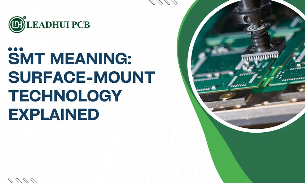
SMT means Surface-Mount Technology: a method of attaching electronic components directly onto the surface of a printed circuit board (PCB). Rather than inserting long component leads through drilled holes, SMT uses small surface-mount components that are placed on solder-coated pads and permanently connected through controlled heating. In practical terms, SMT is what makes modern electronics…
Requisitos de arquivos de PCBA para uma fabricação impecável
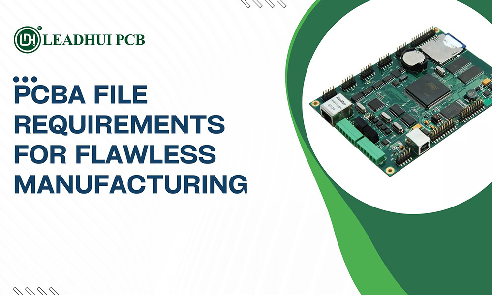
When preparing your printed circuit board design for assembly (PCBA), providing the right manufacturing files is the difference between a smooth product launch and a costly, delayed nightmare. While most Contract Manufacturers (CMs) will hand you a basic checklist asking for a BOM and Gerber files, modern Turnkey PCB Assembly requires far more comprehensive data…