The standard PCB thickness for many general-purpose rigid boards is 1.6 mm nominal finished thickness, approximately 0.063 inch or 63 mil. JLCPCB’s standard PCB thickness guide, updated September 9, 2026, describes 1.6 mm as a common standard thickness. Other dimensions are used too, as described in Altium’s board thickness and stackup guide. A nominal value is a target, not a measurement or an acceptance range. Before selecting one, check the finished board’s tolerance against the actual connector, enclosure and stackup requirements.
Ключевые выводы
- A 1.6 mm nominal thickness is a common starting point for rigid PCBs. The design and fabrication agreement determine the dimension for a particular board.
- Nominal thickness and tolerance define a range. Connector fit needs that range checked at the same measurement surfaces used in the connector drawing.
- Total board thickness, copper thickness and the dielectric spacing between selected layers are different dimensions.
- Document the measurement location, finished surfaces, tolerance and inspection method, then obtain fabrication and engineering approval before release.
What Is the Standard PCB Thickness?
A common standard circuit board thickness is 1.6 mm nominal, but that is a convention rather than a mandatory size for every design. The controlled drawing and the agreed fabrication requirements define the target and acceptable limits for a specific board.
Metric and imperial labels that look similar are not identical:
- 1.60 mm = 0.06299 inch, approximately 63 mil.
- 0.062 inch = 1.5748 mm, approximately 1.57 mm.
- 1/16 inch = 1.5875 mm.
These values may be rounded together in conversation. On a drawing, keep the intended nominal dimension, units and tolerance explicit. The difference can matter when a connector or housing has a restricted clearance.
PCB Thickness Chart: Common Sizes in mm and Mils
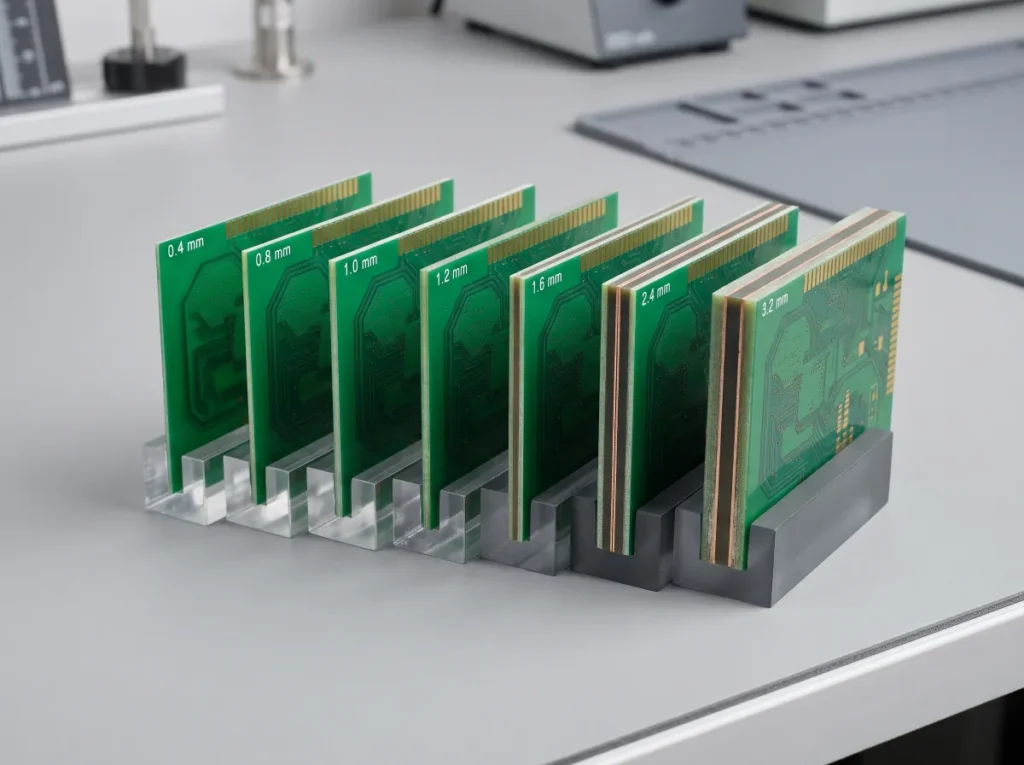
The following nominal board thickness options appear on the PCB manufacturing capabilities page, checked October 29, 2026. The inch and mil values are rounded; one mil is 0.001 inch.
| Номинальная толщина | Approx. inches | Approx. mils | When to consider it |
|---|---|---|---|
| 0,4 мм | 0.0157 | 15.75 | Low-profile layouts; review handling. |
| 0,6 мм | 0.0236 | 23.62 | Thin rigid builds; confirm support. |
| 0,8 мм | 0.0315 | 31.50 | Shallow housings; check deflection. |
| 1,0 мм | 0.0394 | 39.37 | Limited clearance; confirm the stackup. |
| 1,2 мм | 0.0472 | 47.24 | Where the mechanical interface calls for it. |
| 1,6 мм | 0.0630 | 62.99 | A common starting point; confirm fit. |
| 2,0 мм | 0.0787 | 78.74 | Where more stiffness is needed; check drilling. |
| 2.4 mm | 0.0945 | 94.49 | Thicker builds; review slots and via depth. |
| 3.2 mm | 0.1260 | 125.98 | Thicker builds; review drilling and fabrication. |
These are nominal values, not acceptance ranges. A listed size does not establish availability for every material, copper weight or layer count. Confirm the current options and the proposed construction with the fabricator.
What Does Finished PCB Thickness Include?
Finished PCB thickness describes a dimension across the completed board, but the surfaces and measurement location must be defined. A connector may control a different local dimension from the general board thickness on a fabrication drawing.
Board thickness, copper thickness and dielectric spacing
| Dimension | Что он описывает | Почему это важно |
|---|---|---|
| Толщина готовой платы | The complete board between specified surfaces | Connector and enclosure fit |
| Толщина меди | A specified conductive layer | Conductor geometry and fabrication |
| Dielectric spacing | Insulation between particular copper layers | Stackup and impedance calculations |
Copper weight is a separate specification from total board thickness. PCB Prime’s copper conversion reference puts 1 oz of copper per square foot at approximately 35 µm, or 0.035 mm, nominal thickness. Plating can add copper to outer layers, so finished copper can differ from the starting foil.
Where and how is thickness measured?
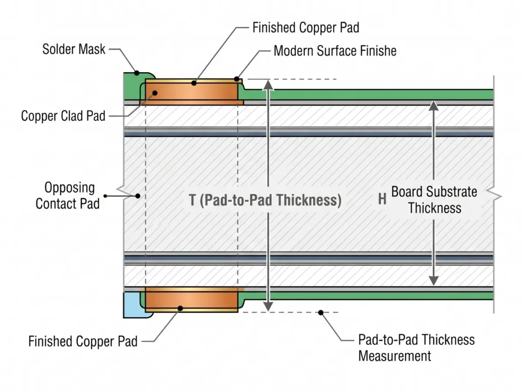
A rigid board’s construction can include cores, prepreg and copper layers. Plating, solder mask and surface finish can also affect a local measurement. Ask which surfaces the fabricator uses for its finished-thickness specification, whether mask and finish are included, and where and how it measures the board.
At a card edge, pad-to-pad thickness is the local distance between the specified finished connector pad surfaces on opposite sides of the board. A reading over solder mask elsewhere does not automatically describe that dimension.
How to Choose PCB Thickness for Your Design
Choose a nominal thickness only after checking the mechanical and fabrication constraints together. Use the actual product drawings and ask the fabricator to review the proposed construction.
| Требование | Design question | Confirmation needed |
|---|---|---|
| Connector or board slot | What card thickness range and surfaces does the drawing specify? | Compare both finished limits at the stated location. |
| Enclosure and mounting | Does the board clear the housing, standoffs and fasteners? | Check the allowed range and assembly clearances. |
| Support and handling | Can the board span its supports and withstand assembly loads? | Review deflection and the handling process. |
| Layer stack | Can the selected layers and dielectric spacings meet the target? | Approve the stackup and any impedance requirements. |
| Vias and drilling | Does board thickness change the hole depth-to-diameter ratio? | Confirm drill and plating feasibility. |
| Materials and supply | Are the materials and construction available at the target thickness? | Confirm options, cost and lead time for the build. |
For otherwise comparable boards, increasing thickness generally increases stiffness. Board dimensions, support span, material, layup and loads also affect deflection. A thin rigid board is not automatically a flex circuit; it should not be treated as one simply because it bends.
Layer count does not uniquely determine finished thickness. A different total thickness may require a stackup revision, but it does not by itself determine an impedance change. Impedance depends on the relevant trace geometry, dielectric spacing and materials. Review the proposed construction with the fabricator and use the руководство по проектированию печатных плат с контролируемым импедансом for the electrical specification. For material selection, see FR-4 PCB materials and design.
Worked Example: Will a 1.6 mm Board Fit a Card-Edge Connector?
A PCB thickness tolerance must be compared with the connector’s full permitted card range at the same surfaces. The following educational example combines a real connector drawing with a separate supplier’s published board tolerance. It is not a measured customer design or a qualification result.
Read the connector drawing
Этот Чертёж Samtec HTEC8, редакция N, полученный 29 октября 2026 года, указывает вариант толщины карты -01 с номинальной толщиной сопрягаемой карты 1.57 мм и допуском между контактными площадками ±0.157 мм . Расчётные пределы составляют:
1.57 – 0.157 = 1.413 мм минимум; 1.57 + 0.157 = 1.727 мм максимум.
На чертеже серии также указан другой вариант толщины карты. Прежде чем использовать эти значения, проверьте точную модель разъёма, актуальную редакцию чертежа, заходную часть и все остальные требования к сопряжению.
Сравните полный диапазон толщины платы
В качестве отдельного примера поставщика на странице JLCPCB с техническими возможностями, проверенной 29 октября 2026 года, указан допуск толщины ±10% для плат толщиной не менее 1.0 мм. Применение этого иллюстративного допуска к плате с номинальной толщиной 1.60 мм даёт:
1.60 × 0.90 = 1.44 мм минимум; 1.60 × 1.10 = 1.76 мм максимум.
Если бы этот допуск толщины платы распространялся на те же поверхности между контактными площадками на сопрягаемом крае, его верхний предел 1.76 мм превышал бы верхний предел разъёма 1.727 мм на 0.033 мм. Его нижний предел 1.44 мм был бы на 0.027 мм выше минимального значения для разъёма. При таком условии одного допуска платы недостаточно, чтобы гарантировать соответствие всего допустимого диапазона толщины платы диапазону толщины разъёма.
Страница поставщика не подтверждает, что указанный допуск толщины относится к этим поверхностям между контактными площадками. Прежде чем сравнивать физические требования, выясните, как именно выполняются измерения. Ни опубликованные значения, ни этот расчёт не доказывают, что конкретная изготовленная карта соответствует требованиям или не соответствует им.
Зафиксируйте возможную спецификацию и открытые вопросы
Один из гипотетических запросов — 1.57 мм ±0.10 мм между контактными площадками на сопрягаемом крае, что даёт диапазон от 1.47 до 1.67 мм. На тех же определённых поверхностях запрошенный диапазон находится внутри указанного диапазона разъёма с запасом 0.057 мм на каждом пределе.
| Требование | Пример диапазона | Статус |
|---|---|---|
| Сопрягаемая карта HTEC8 -01 | от 1.413 до 1.727 мм между контактными площадками | Опубликованный чертёж разъёма; проверьте редакцию и другие требования. |
| Иллюстративный пример платы 1.60 мм с допуском ±10% | от 1.44 до 1.76 мм | Пример опубликованного допуска; соответствие размера между контактными площадками не подтверждено. |
| Предлагаемая плата 1.57 мм с допуском ±0.10 мм | от 1.47 до 1.67 мм между контактными площадками | Гипотетический запрос; согласование изготовления и контроля ещё не завершено. |
Предлагаемый допуск не является опубликованной возможностью изготовителя. Убедитесь, что плату можно изготовить и проверить с таким допуском, согласуйте порядок учёта покрытия и неопределённости измерений и получите одобрение проектировщика и изготовителя. Само по себе попадание одного диапазона в другой не подтверждает полную совместимость с разъёмом.
Укажите толщину печатной платы на чертеже для изготовления
На чертеже для изготовления следует указать как требование к толщине готовой печатной платы, так и способ его проверки. Укажите номинальный размер и единицы измерения, допуск или явные предельные значения, область и поверхности измерения, требуемую отделку и покрытия, а также соответствующий метод контроля. Если используется сопрягаемый край, укажите модель и редакцию разъёма.
Для приведённого выше гипотетического примера возможна такая примечание:
На сопрягаемом крае разъёма требуется толщина 1.57 мм ±0.10 мм, измеренная между контактными площадками на готовых контактных поверхностях. Места и метод измерения, а также порядок учёта неопределённости подлежат согласованию и инженерному утверждению.
Используйте это примечание только после проверки требований к разъёму и чертежа для изготовления. При необходимости отдельно укажите общую толщину платы, включая соответствующие поверхности и допуск; не предполагайте, что она совпадает с локальным размером между контактными площадками. Зафиксируйте материал, медь и утверждённый стек слоёв, а также требуйте согласования изменений, влияющих на спецификацию. Убедитесь, что чертёж, стек слоёв и требования к разъёму согласованы во всех контролируемых документах. Документ Контрольный список по DFM для печатных плат охватывает более широкий комплект документации для выпуска.
Если в проекте используются документы IPC, проверьте применимые редакции и положения. IPC-2221 рассматривает общие вопросы проектирования печатных плат, IPC-2222 — проектирование жёстких плат на органической основе, а IPC-6012 — квалификацию и эксплуатационные характеристики жёстких плат. Таблица редакций документов IPC помогает определить редакции; одного номера документа недостаточно, чтобы задать допуск для вашей платы.
Распространённые ошибки при задании толщины печатной платы
- Считать номинальное значение гарантией точного сопряжения. Сравнивайте согласованные минимальное и максимальное значения с предельными значениями сопрягаемой детали.
- Считать 0.062 дюйма и 1.60 мм одинаковыми значениями на чертеже. Preserve the actual dimension and units through the release package.
- Confusing copper weight with board thickness. Specify each copper layer separately from the finished board dimension.
- Comparing different surfaces. Establish whether both requirements refer to finished pads, solder mask or another defined surface.
- Assigning one thickness to each layer count. Ask for a buildable stackup that meets the target and tolerance.
- Changing the stackup without a review. Recheck mechanical fit and any controlled impedance requirements before approving the change.
PCB Thickness FAQ
How thick is an FR-4 PCB?
A common FR-4 PCB thickness is 1.6 mm nominal, but FR-4 boards can use other dimensions. Select one for the mechanical interfaces and layer construction, then agree the finished thickness and tolerance with the fabricator.
Is 1.6 mm the same as 0.062 inch?
No. They are close, but 0.062 inch equals 1.5748 mm. Use the exact nominal dimension and tolerance on the drawing when checking fit or placing an order.
What is the tolerance for a 1.6 mm PCB?
It depends on the fabrication agreement and how the dimension is measured. The ±10% example above comes from a cited supplier’s published conditions; it is not a universal tolerance or a guarantee for another fabricator.
How thick is 1 oz of copper?
One ounce of copper per square foot corresponds to approximately 35 µm nominal copper thickness. That describes copper, not the entire PCB. Finished outer-layer copper can differ from the starting foil after plating.
Plan Your Fabrication Review
Choose a thickness whose agreed range meets the mechanical requirements, then confirm the stackup and measurement surfaces. For a project-specific review, share your board files, required finished thickness, connector drawing and proposed stackup through rigid PCB manufacturing.