Блог
Здесь вы сможете получить профессиональные знания, охватывающие весь процесс от проектирования печатных плат до их сборки, а также ознакомиться с подробным анализом последних тенденций в электронной промышленности.
Industrial PCB Production: Process & QA
Industrial PCB production turns an approved circuit-board design into bare boards and, when ordered, populated assemblies for industrial equipment. The route includes fabrication, component assembly, inspection and agreed testing. Approval depends on the specified build, operating conditions and acceptance criteria. A motor controller, sensor interface and cabinet-mounted control board can require different materials, mechanical support…
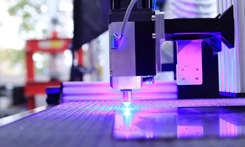
Алюминиевая печатная плата: тепловая конструкция и материалы
An aluminum PCB is a printed circuit board that combines copper circuitry, an electrically insulating thermal dielectric and an aluminum base. The dielectric carries heat toward the metal while separating the circuit electrically. This construction is useful for LED lighting and power electronics when the board, mounting interface and cooling surface form a suitable heat…
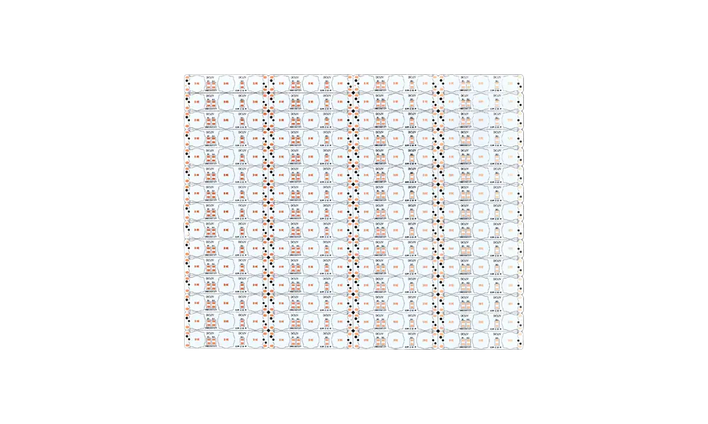
Печатная плата HDI: структура слоёв, микропереходы и конструкция
An HDI PCB, or high-density interconnect printed circuit board, uses fine conductors and compact interlayer connections to fit more wiring into a given area. Laser-drilled microvias and thin buildup layers help connect dense component pads without using a full-thickness hole at every connection. The design question is whether those features solve a routing constraint worth…

Жёсткая печатная плата: материалы, конструкция и варианты дизайна
A rigid PCB, or rigid printed circuit board, supports components and connects them through copper conductors on a substrate designed to retain its shape in service. It suits electronics whose circuitry stays fixed within an enclosure, rather than bending during use. Choosing one means matching its construction to the circuit, mounting, connectors and environment. Layer…

Гибкая печатная плата: типы, материалы, структура слоёв и правила проектирования
A flex PCB is a circuit built on a flexible polymer film, usually polyimide, with copper conductors bonded to it and a coverlay protecting them. That is the definition, and it is the part already answered above the search results. It is not the part that decides whether your build works. Four questions decide that,…
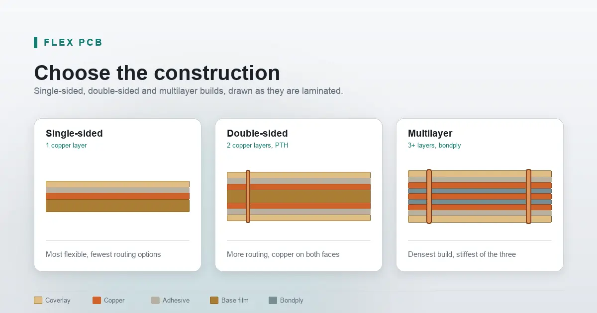
Радиус изгиба гибкой печатной платы: как его рассчитать и задать
You have a stackup, a housing envelope, and a mechanical engineer asking for a flex PCB bend radius. The answer is not a lookup table; it is a strain calculation, and the multipliers in the tables are what that calculation returns once you fix a stackup. Every published multiplier, whether it reads 6×, 10×, 12×,…
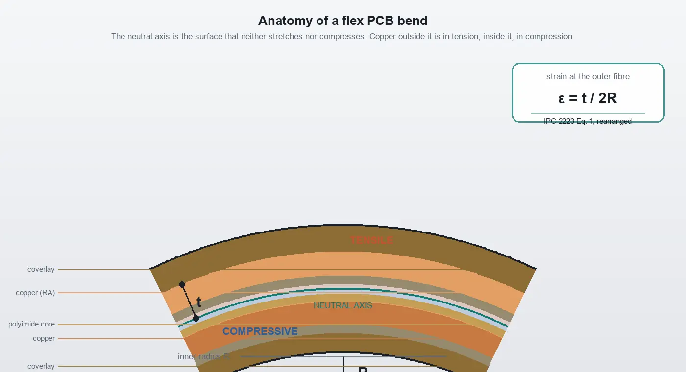
Руководство по пайке оплавлением: процесс, профиль и дефекты
Reflow soldering is the process that attaches surface-mount components to a printed circuit board by heating stencilled solder paste until it melts, wets the component terminations and forms the joint on cooling. It is the primary assembly method for almost every modern electronic product, and it is the step where the most expensive mistakes become…
Что такое Solder Paste Inspection (SPI)? Измерения, дефекты и контроль качества
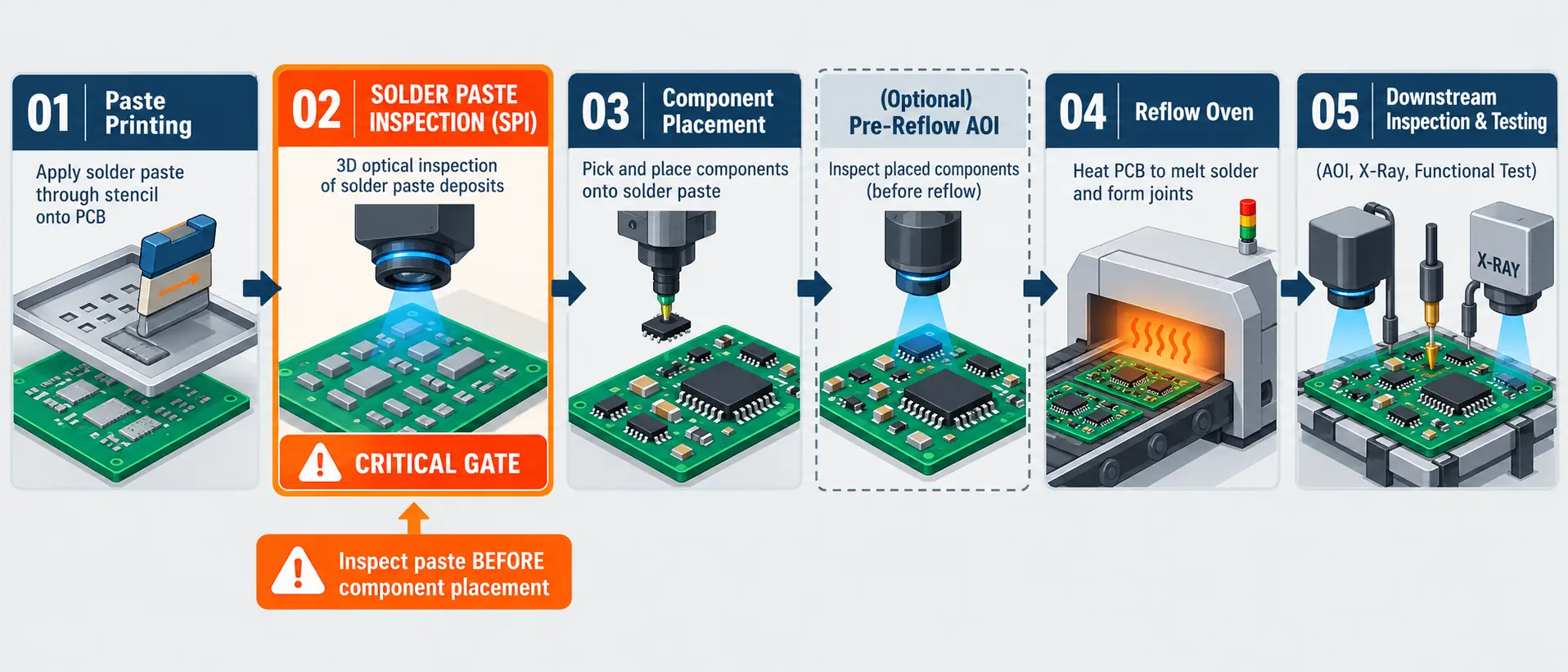
Solder paste inspection (SPI) checks paste deposited on a PCB after printing and before component placement. A 3D SPI system measures deposit volume, height, area, and alignment against programmed limits. It allows defective prints to be held and corrected before placement and reflow. For hardware engineers and PCBA buyers, the key decision is whether the…
10 лучших программ для проектирования PCB в 2026 году
KiCad is the strongest free desktop starting point for engineers choosing PCB design software in 2026. Altium Designer through Altium Develop is a strong paid choice for small teams that want shared libraries, browser review, and electrical–mechanical collaboration in one connected workflow. Both support serious board design; the purchasing decision is whether the surrounding workflow…
Руководство по SMD-резисторам: маркировка, размеры, посадочные места и ограничения
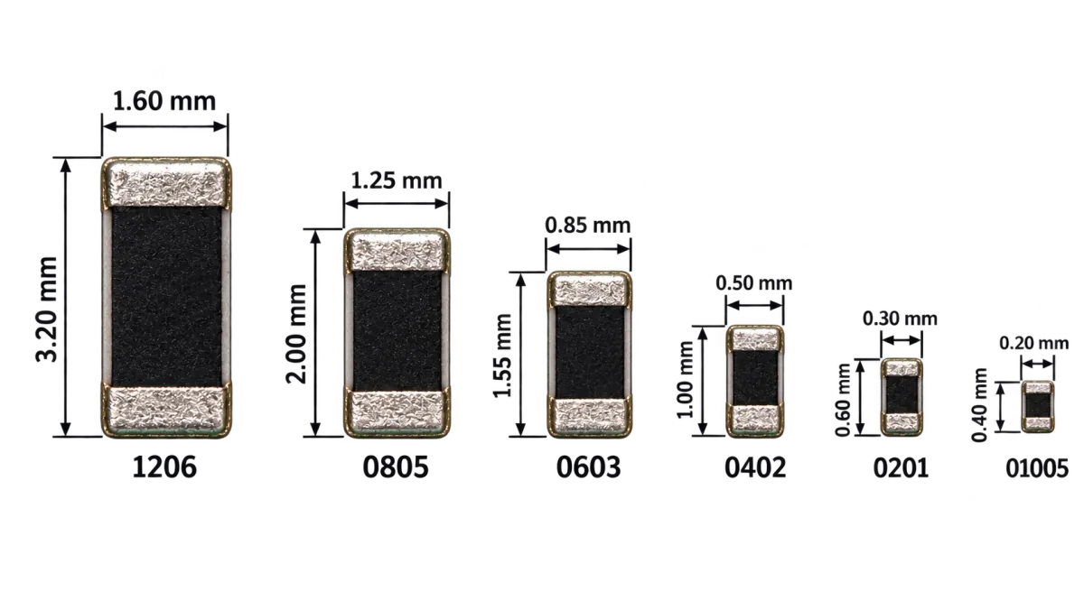
An SMD resistor is a fixed-value resistor in a leadless rectangular package that solders to pads on the surface of a printed circuit board rather than passing through holes. It is typically the most numerous component on a board, and the one most often specified from habit rather than from the datasheet. Most guides to…
Медно-фольгированный ламинат (CCL): типы, производство, характеристики и стандарты
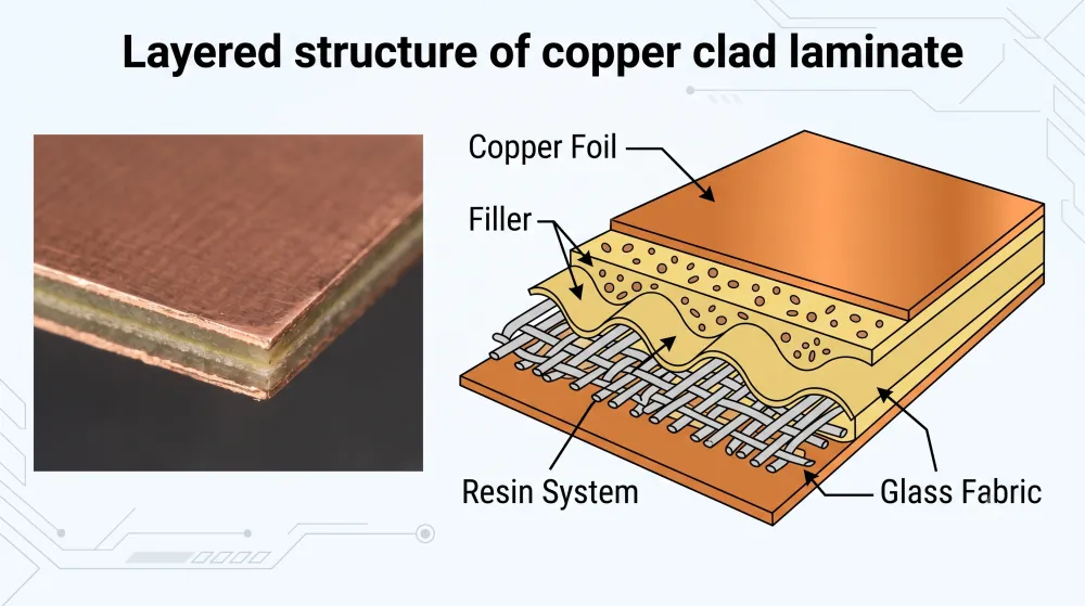
Copper clad laminate, or CCL, is a base material from which PCB conductors are formed. It consists of copper foil bonded to an insulating material such as cured glass-reinforced epoxy, a flexible polymer film, or a thermally conductive dielectric on a metal base. In a conventional multilayer rigid PCB, patterned CCL commonly becomes a core.…
JLCPCB против PCBWay: какой производитель печатных плат подходит для вашего проекта? (2026)
For a straightforward PCB prototype or a small assembly order that fits JLCPCB’s Economic PCBA rules, start with JLCPCB, especially when the components are already in its inventory. For rigid-flex or extensive custom fabrication requirements, shortlist PCBWay early. These recommendations follow from JLCPCB’s economical assembly tier and PCBWay’s documented advanced manufacturing options. The JLCPCB vs…

Что такое GND? Объяснение смысла, типов и заземления печатной платы
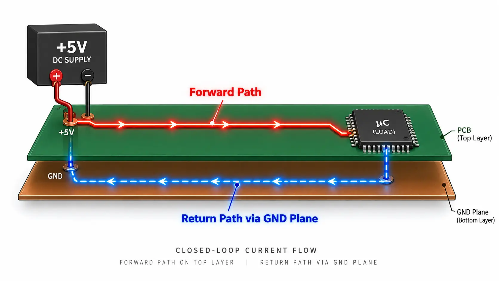
GND appears on almost every circuit diagram, PCB, power supply, and electronic module. It is often described as “zero volts” or “the negative terminal,” but neither description is universally correct. In electronics, GND stands for ground. It is the reference node against which other voltages are measured and, in many circuits, part of the path…
Что такое сквозное отверстие? Типы, использование и руководство по проектированию
A through hole is an opening that passes completely from one side of a printed circuit board (PCB) to the other. It may be plated with conductive copper to create an electrical connection, or left unplated for mechanical use. Through holes are commonly used for component leads, connectors, vias, mounting hardware, alignment pins, and slots.…

Что такое пакеты QFN? Практическое руководство по проектированию и сборке печатных плат
Корпуса QFN встречаются повсюду: от источников питания и беспроводных модулей до датчиков, микроконтроллеров и автомобильной электроники. Их малые габариты, короткие электрические пути и эффективный отвод тепла делают их привлекательной альтернативой более крупным корпусам с выводами. Однако те же нижние соединения, которые экономят место, делают проектирование посадочного места, пайку и контроль QFN менее щадящими. Итак,…

Руководство по материалу печатных плат: типы, свойства и выбор
Материал печатной платы влияет не только на физическую прочность платы. Он определяет импеданс, потери сигнала, рассеивание тепла, размерную стабильность, надежность сборки, технологичность, сроки изготовления и стоимость. Материал, который хорошо подходит для простого контроллера, может оказаться непригодным для радарного модуля на 77 ГГц, платы светодиодов с высоким током или жестко-гибкого медицинского устройства.…

Конструкция печатной платы с контролируемым импедансом: стек, спецификации и тестирование
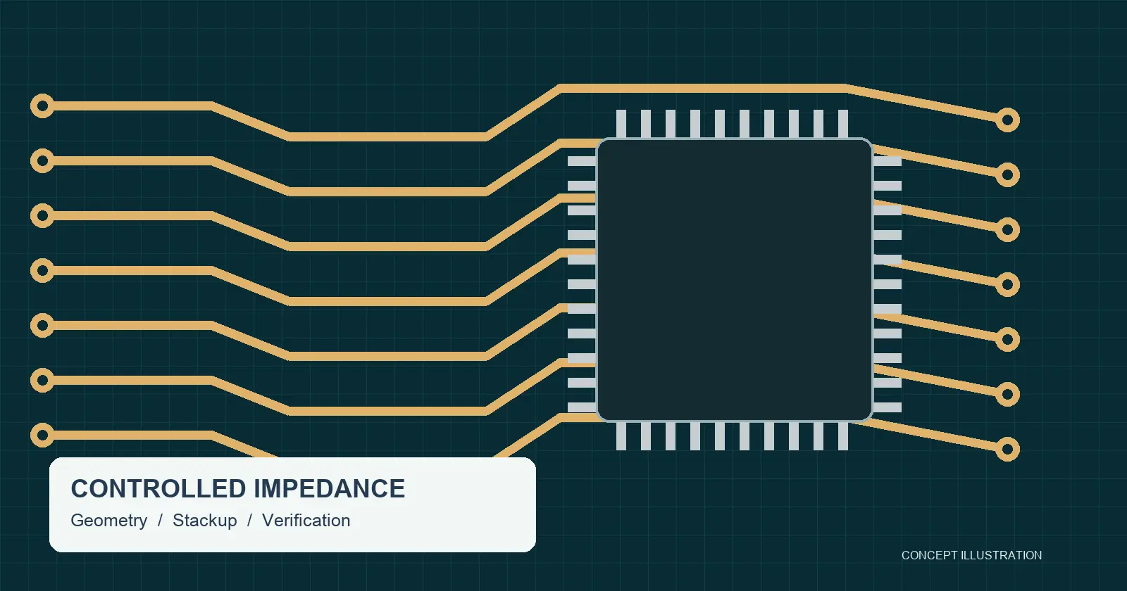
Controlled impedance is the practice of designing and manufacturing PCB traces so their characteristic impedance meets a specified target and tolerance. The result depends on the conductor geometry, dielectric construction, and reference planes. A complete requirement also states how the manufacturer will verify the finished structure. A note that says only “50 ohms” leaves important…
Резистор 10к: Цветовая маркировка, применение и как выбрать правильный
Резистор 10 кОм — это пассивный электрический компонент с номинальным сопротивлением 10 000 Ом (10 кОм). В современном проектировании схем это одно из самых распространенных значений, встречающихся как на макетных платах, так и на серийных печатных платах. Инженеры и любители обращаются к резисторам 10 кОм, поскольку они представляют собой идеальную электрическую золотую середину: они ограничивают ток до безопасного,…

Проектирование печатной антенны: топология, материалы и производство
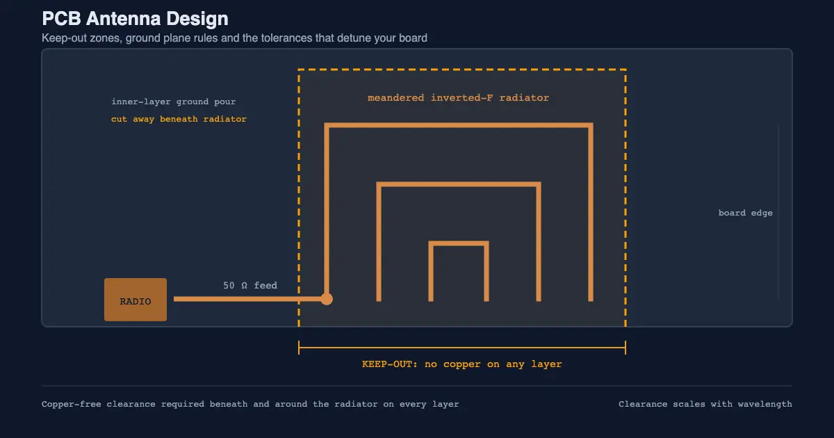
A PCB antenna is a copper trace or pattern etched directly onto a printed circuit board that transmits and receives radio frequency electromagnetic waves. It is the cheapest way to give a product wireless connectivity, because it adds no connector, no cable and no bill-of-materials line. It is also the part of a design most…
Анод и катод светодиода: как определить положительный и отрицательный выводы
Светодиод (LED) — это поляризованное полупроводниковое устройство, которое пропускает ток только в одном направлении. Чтобы зажечь светодиод, необходимо правильно подключить его положительный и отрицательный выводы в вашей цепи. На стандартных светодиодах с выводами для монтажа в отверстия более длинная ножка и закругленная сторона представляют анод, а более короткая ножка и…