Solder paste inspection (SPI) checks paste deposited on a PCB after printing and before component placement. A 3D SPI system measures deposit volume, height, area, and alignment against programmed limits. It allows defective prints to be held and corrected before placement and reflow. For hardware engineers and PCBA buyers, the key decision is whether the assembler can measure the relevant deposits reliably and act on failures consistently.
Passing SPI confirms that inspected deposits meet those limits. It does not certify finished solder joints or electrical functionality.
Key takeaways
- Inspect after printing and before placement, while deposits remain accessible.
- Interpret percentages against a documented nominal volume and qualified acceptance limits.
- Evaluate failed-print containment, correction, and reinspection alongside equipment capability.
- Retain downstream inspection and testing for defects paste measurement cannot establish.
The process sequence is paste printing → SPI → component placement → reflow → downstream inspection and testing. Pre-reflow AOI may also follow placement.
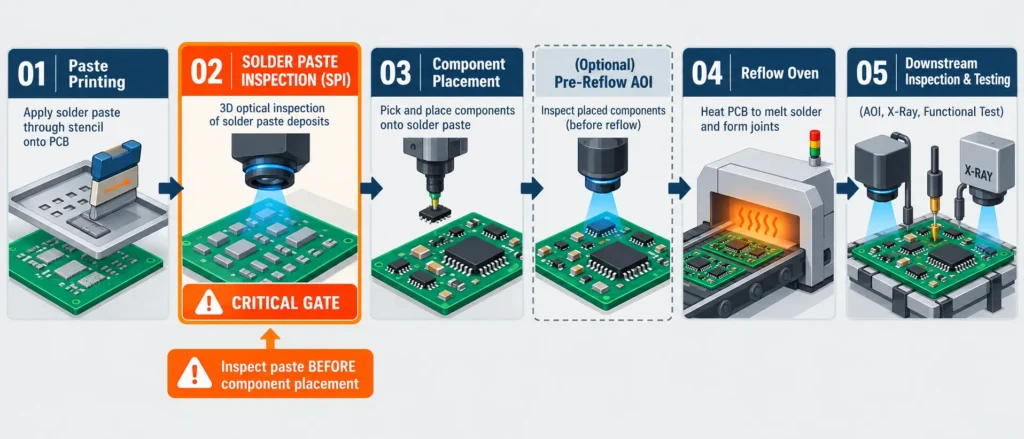
What does SPI measure, and how does 3D inspection work?
SPI evaluates the geometry and position of printed paste. Its usefulness comes from comparing those measurements with the intended deposit, using the correct board and stencil revisions.
Read the measurements in an SPI result
Volume, height, area, and offset describe different aspects of a deposit; none should be interpreted without its reference.
| Measurement | Meaning | Useful reporting basis |
|---|---|---|
| Volume | Integrated paste volume above the local reference surface | mm³ or nL; percentage of a stated nominal volume |
| Height | Deposit height relative to the reference surface | µm; identify mean, maximum, or other reported statistic |
| Area | Deposit footprint in the inspection region | mm²; percentage of the programmed reference area |
| X/Y offset | Displacement from the intended deposit location | Signed µm along each board axis |
| Shape/bridging | Irregular geometry or paste connecting adjacent regions | Annotated image and the applicable detection rule |
Commercial SPI systems inspect these geometric features, although available outputs vary by configuration.
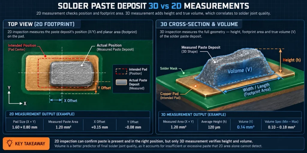
Two deposits can cover similar areas but contain different volumes. A thin deposit may look complete from above while providing less paste than intended. Conversely, a tall central peak does not prove adequate volume across the footprint.
Understand what 3D adds to 2D inspection
Three-dimensional inspection adds measured height and volume to surface-image information. Two-dimensional checks can evaluate presence, area, position, and visible paste connections, but cannot establish integrated three-dimensional volume from footprint alone.
The system aligns the inspection program to the PCB, captures the deposits, reconstructs their surfaces, and compares calculated measurements with limits. Yamaha, for example, documents contour extraction with 2D lighting followed by phase-shift height measurement. That is one implementation, not a description of every SPI machine.
Use 3D measurement when the production decision requires quantitative volume or height. Adequacy still requires validation on the actual deposit sizes, surfaces, and board conditions.
Which printing defects can SPI flag before they become assembly problems?
SPI can flag missing, insufficient, excessive, shifted, or connected paste deposits. These findings indicate printing abnormalities and downstream risks; they do not guarantee a particular reflow defect.
Connect paste abnormalities to the next investigation
The location and pattern of an alarm determine the first investigation. A recurring low deposit at one aperture suggests a different problem from a uniform offset across the panel.
| Printed-paste condition | SPI evidence | Possible downstream risk | First investigation | Required qualification |
|---|---|---|---|---|
| Insufficient deposit | Volume in nL/mm³ and % of stated nominal | Insufficient joint solder or open connection | Aperture blockage, release, paste condition | Aperture geometry, local thickness, paste product |
| Excess deposit | Volume plus area and shape | Bridging or excess solder | Intended aperture volume and print settings | Package spacing and deposit design |
| Offset | Signed X/Y displacement in µm | Reduced termination overlap | Registration, fiducials, board support | Direction-specific limits and reference |
| Paste bridge | Image showing connected deposits | Solder-bridge risk | Stencil underside cleanliness and alignment | Gap geometry and image segmentation |
| Missing deposit | Image and measured/detection result | Missing or insufficient solder | Blocked aperture and failed transfer | Detection floor and inspection-region accuracy |
| Paired-pad imbalance | Both volumes and a defined comparison | Contributor to asymmetric soldering or tombstoning | Print balance, layout, placement, thermal conditions | Defined imbalance formula and validated relevance |
These are investigation candidates. Changing a printer setting without confirming the pattern can disturb otherwise acceptable deposits.
Inspecting before placement preserves access to the paste and avoids adding components to an unresolved print. Cleaning and reprinting may still consume labor and materials, but the response can occur before component removal or solder-joint repair is necessary.
Separate a printing warning from a finished-joint diagnosis
SPI cannot directly establish post-reflow void percentage, wetting, joint strength, or continuity. It examines exposed paste before the joint exists.
Tombstoning illustrates the boundary. Unequal deposits can contribute, but pad geometry, component position, alloy behavior, and wetting forces also influence the outcome. Indium identifies several of these interacting factors.
A paste alarm warrants review; it is not a completed-joint diagnosis. Likewise, a passing print cannot exclude placement or reflow problems that occur later.
How should solder paste volume and inspection limits be defined?
A meaningful SPI result requires a defined nominal deposit, capable measurement, and approved limits appropriate to the assembly. A percentage without its denominator is incomplete.
Define what “100% paste volume” means
For a straight-sided stencil aperture, the geometric volume reference is aperture area × local stencil thickness. IPC-7527 defines designed volume on this basis. Use local thickness for a step stencil and the actual aperture geometry rather than assuming the copper pad and aperture are identical.
Transfer efficiency expresses deposited volume relative to aperture volume.
Transfer efficiency (%) = measured deposit volume ÷ aperture volume × 100
Consider this illustrative calculation:
| Parameter | Value |
|---|---|
| Rectangular aperture | 0.30 × 0.30 mm |
| Local stencil thickness | 0.10 mm |
| Calculated aperture volume | 0.009 mm³ = 9 nL |
| Measured deposit volume | 0.0072 mm³ = 7.2 nL |
| Transfer efficiency | 80% |
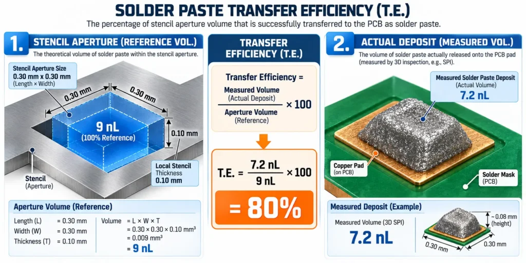
The calculation establishes a ratio, not a pass/fail decision. Confirm whether the machine’s percentage uses this aperture volume or another programmed nominal value. Paste volume also includes flux; it is not the final metallic solder volume after reflow.
Qualify limits against the actual printing process
Limits must distinguish unacceptable deposits from acceptable variation under the qualified process. Start with aperture geometry, stencil thickness, package risk, pad spacing, board support, and the measurement reference. Record the paste product, alloy, powder type, flux system, and handling conditions.
Material conditions are product-specific. Kester’s October 2021 NP560 datasheet, for example, lists an eight-hour stencil life at 65–85 °F and 10–70% relative humidity. That is guidance for the named material under stated conditions, not a universal paste-life rule or SPI acceptance window.
Resolution describes the smallest distinguishable measurement change; repeatability concerns agreement under repeated conditions; accuracy concerns agreement with a reference. Yamaha lists 1 µm height resolution for its YSi-SP, which does not establish 1 µm accuracy on production deposits.
First-article evaluation and measurement-system analysis should support the selected limits. Keep acceptance limits separate from statistical control limits used to detect process changes. Capability indices require a stable process and suitable data; combining unrelated deposit families can conceal variation.
Do not treat one volume window or Cpk target as an IPC requirement for every pad.
Near a decision limit, measurement variation can produce false rejects or missed abnormalities. Evaluate repeatability on representative deposits, including reloading and alignment where relevant. A calibration target check alone does not demonstrate capability across every production geometry.
What should happen when a board fails SPI?
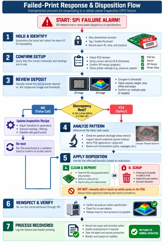
A failed SPI result should prevent routine release to placement until the alarm has been reviewed and the board has an authorized disposition. Correction must address both the affected board and any recurring printing problem.
Follow a controlled response to the alarm
The response begins with containment, then separates measurement error from a real print abnormality.
- Hold and identify the board. Retain the board/panel identity, alarm location, and original result. Prevent accidental transfer to placement.
- Confirm the inspection setup. Check PCB and stencil revisions, recipe, fiducial alignment, support, and local height reference.
- Review the deposit. Compare the image and measurements with the approved limits. Route ambiguous calls to qualified review rather than dismissing them automatically.
- Classify the pattern. Determine whether the issue follows one aperture, a board region, the full panel, print direction, or elapsed production time.
- Investigate the corresponding variables. Examine blockage, stencil underside condition, registration, release, paste condition, and support as indicated by the pattern.
- Apply the approved disposition. Use compatible cleaning and reprinting, a qualified correction method, or scrap as appropriate. Do not assume wiping the board or adding paste manually is acceptable.
- Reinspect and confirm recovery. Verify the corrected board and subsequent prints according to the control plan before normal release resumes.
IPC-7526 addresses stencil and misprinted-board cleaning; the applicable procedure must also account for the paste, PCB materials, cleaning chemistry, and drying requirements.
Confirm that the process recovered
Recovery means that corrective action restored the intended process, with evidence retained. Preserve the original alarm, reviewer decision, reason, action, recipe revision, and final disposition.
Examine subsequent results for the affected aperture or deposit family. Widening a limit until alarms disappear does not establish recovery; any limit change needs a technical basis and approval.
Automatic printer feedback can support control, but it must be configured and validated. Yamaha documents offset feedback and cleaning-cycle functions. Their availability on a platform does not prove they are enabled on a particular assembly line.
How do SPI, AOI, X-ray, and electrical tests work together?
These methods address different stages and failure mechanisms. SPI controls printing; later inspection and tests evaluate conditions that do not yet exist or cannot be observed at SPI.
| Method | Production stage | Evidence obtained | What it cannot establish alone |
|---|---|---|---|
| 2D SPI | After print, before placement | Paste presence, area, position, visible connections | Integrated three-dimensional paste volume |
| 3D SPI | After print, before placement | Paste height, volume, area, offset, shape | Finished-joint or circuit conformity |
| AOI | After placement and/or reflow | Programmed component and accessible solder-feature checks | All hidden-joint conditions |
| X-ray/AXI | Usually after reflow | Selected internal solder features, including voids or bridges | Complete electrical functionality |
| Electrical/functional testing | Defined assembly-test stage | Tested connections, circuit responses, or functions | Every physical or latent defect |
Omron describes SPI before placement, with optical inspection after placement and reflow. Its CT inspection documentation addresses hidden joints that optical inspection cannot access.
Electrical methods also differ: ICT and flying probe can verify selected circuit properties, while functional testing exercises specified operating behavior. Coverage follows the test design and available access.
Select the combination around assembly risks and customer requirements. A passing inspection sequence is evidence of conformity within its coverage, not proof of every aspect of long-term reliability.
What SPI evidence should you request with a turnkey PCBA quote?
A useful supplier evaluation connects inspection coverage, approved limits, and failure handling to your assembly. A machine name or a generic “SPI included” statement leaves those decisions unresolved.
Request evidence that prevents specific sourcing mistakes
Representative records and a defined control plan show what the supplier measures and how results affect production release. The evidence should address the deposit geometries and board conditions relevant to your project.
| Evidence | Request | Purchasing error prevented |
|---|---|---|
| Inspection coverage | All boards/panels or sampling; inspected sides, deposits, and exclusions | Assuming every board inspected means every relevant deposit covered |
| Approved limits | Nominal reference, deposit-family limits, approval basis, revision | Comparing percentages with different denominators or unqualified limits |
| Measurement capability | Relevant configuration, calibration verification, repeatability and measurement-system evidence | Treating pixel size or resolution as demonstrated accuracy |
| Failed-print disposition | Hold/release authority, correction procedure, reinspection requirements | Accepting alarms that operators routinely bypass |
| Traceability | Board/panel identity linked to recipe, stencil revision, result, and disposition | Receiving a report that cannot be connected to the supplied lot |
| Reporting scope | Available measurements, images, trends, export format, and retention period | Expecting records that were neither collected nor retained |
An anonymized example should retain units, nominal values, approved limits, alarm locations, and dispositions. A pass-rate screenshot alone cannot show whether exclusions or overrides affected coverage.
Record acceptance requirements separately from process-monitoring targets. J-STD-001 addresses soldered-assembly requirements, while IPC-A-610 addresses assembly acceptability; neither name alone specifies your inspection program. State the contractual editions, class, and customer exceptions.
Turn the quality requirement into an actionable RFQ
An actionable RFQ combines matching design files with the required inspection and reporting scope. Supply Gerber and paste-layer data, BOM, CPL/pick-and-place file, assembly drawing, quantity, and critical package details. Include applicable workmanship requirements and electrical or functional test instructions.
Identify deposits or packages needing special review, such as small apertures, closely spaced terminations, or segmented thermal-pad prints. The assembler can then evaluate the stencil and inspection plan together.
LEADHUI lists SPI among its quality and testing capabilities. Confirm coverage, approved limits, reporting, and any exclusions for the quoted build; capability does not establish identical scope for every order.
Clarify whether setup, inspection, and reporting are included or separately quoted. These are project-specific commercial terms, not a standard per-board SPI price.
For a turnkey PCB assembly quote, submit the design package with the critical packages and required records identified. Ask for the proposed inspection plan alongside the build quotation.
Does a prototype need the same SPI coverage as production?
Prototype inspection should follow defect risk and the purpose of the build. A small order does not automatically justify reduced coverage, especially when components are expensive or printing fine features is unproven.
A prototype intended to qualify a production process benefits from comparable paste measurements and traceable results. A simpler development board may support a different documented route if it addresses the relevant risks. Package pitch alone is not a universal selection threshold.
For the next build, define the critical deposits, required evidence, and failed-print response before approving the manufacturing scope. This makes the inspection requirement reviewable before boards enter production.