Blog
Aquí podrá adquirir conocimientos especializados que abarcan toda la cadena, desde el diseño de placas de circuito impreso hasta el montaje, así como un análisis detallado de las últimas tendencias en el sector de la electrónica.
Producción industrial de PCB: proceso y control de calidad
Industrial PCB production turns an approved circuit-board design into bare boards and, when ordered, populated assemblies for industrial equipment. The route includes fabrication, component assembly, inspection and agreed testing. Approval depends on the specified build, operating conditions and acceptance criteria. A motor controller, sensor interface and cabinet-mounted control board can require different materials, mechanical support…
PCB de aluminio: diseño térmico y materiales
An aluminum PCB is a printed circuit board that combines copper circuitry, an electrically insulating thermal dielectric and an aluminum base. The dielectric carries heat toward the metal while separating the circuit electrically. This construction is useful for LED lighting and power electronics when the board, mounting interface and cooling surface form a suitable heat…
PCB HDI: apilado, microvías y diseño
An HDI PCB, or high-density interconnect printed circuit board, uses fine conductors and compact interlayer connections to fit more wiring into a given area. Laser-drilled microvias and thin buildup layers help connect dense component pads without using a full-thickness hole at every connection. The design question is whether those features solve a routing constraint worth…

PCB rígido: materiales, construcción y decisiones de diseño
A rigid PCB, or rigid printed circuit board, supports components and connects them through copper conductors on a substrate designed to retain its shape in service. It suits electronics whose circuitry stays fixed within an enclosure, rather than bending during use. Choosing one means matching its construction to the circuit, mounting, connectors and environment. Layer…

PCB flexible: tipos, materiales, apilado y reglas de diseño
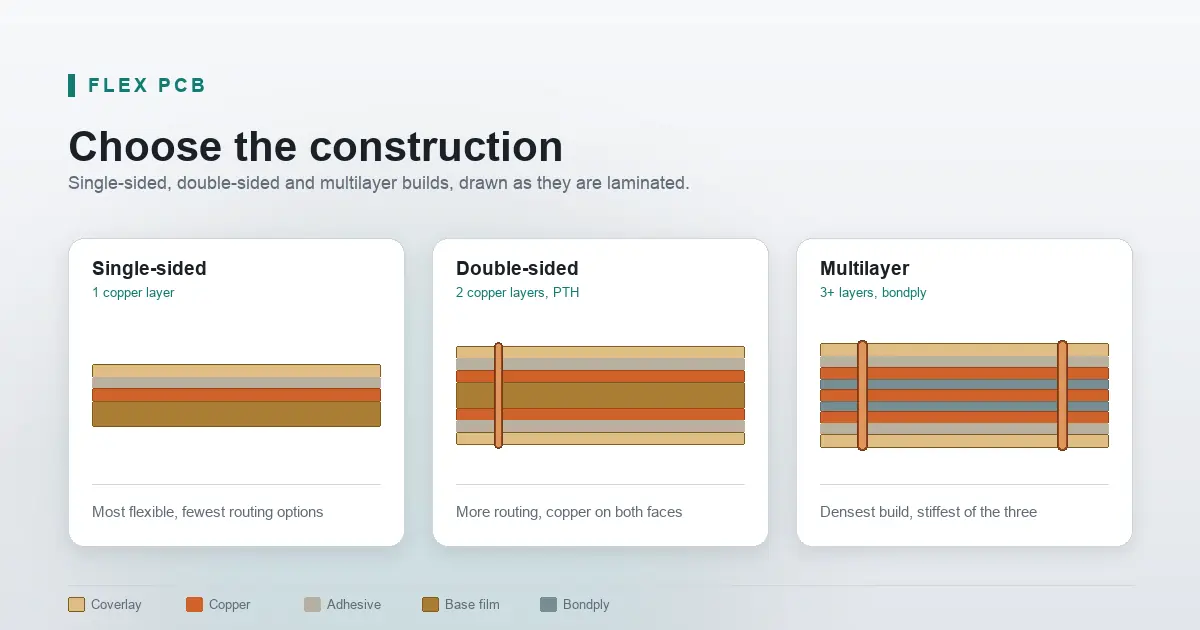
A flex PCB is a circuit built on a flexible polymer film, usually polyimide, with copper conductors bonded to it and a coverlay protecting them. That is the definition, and it is the part already answered above the search results. It is not the part that decides whether your build works. Four questions decide that,…
Radio de curvatura de un PCB flexible: cómo calcularlo y especificarlo
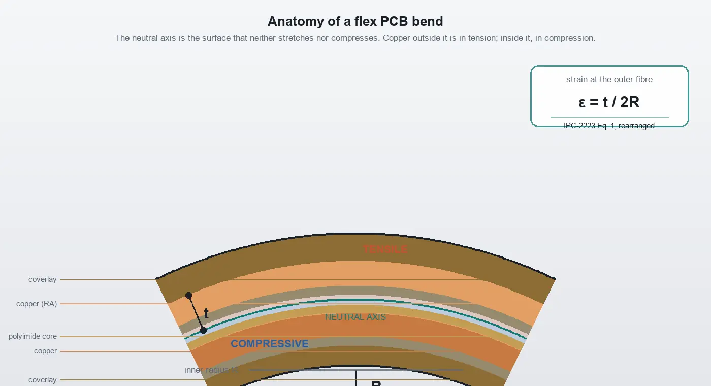
You have a stackup, a housing envelope, and a mechanical engineer asking for a flex PCB bend radius. The answer is not a lookup table; it is a strain calculation, and the multipliers in the tables are what that calculation returns once you fix a stackup. Every published multiplier, whether it reads 6×, 10×, 12×,…
Guía de soldadura por reflujo: proceso, perfil y defectos
Reflow soldering is the process that attaches surface-mount components to a printed circuit board by heating stencilled solder paste until it melts, wets the component terminations and forms the joint on cooling. It is the primary assembly method for almost every modern electronic product, and it is the step where the most expensive mistakes become…
¿Qué es la inspección de pasta de soldadura (SPI)? Mediciones, defectos y Control de calidad
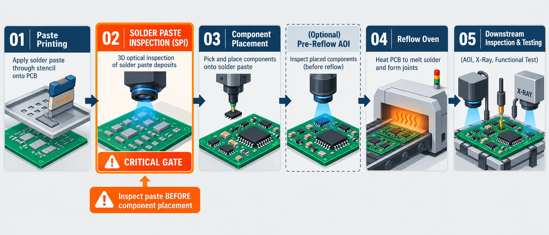
Solder paste inspection (SPI) checks paste deposited on a PCB after printing and before component placement. A 3D SPI system measures deposit volume, height, area, and alignment against programmed limits. It allows defective prints to be held and corrected before placement and reflow. For hardware engineers and PCBA buyers, the key decision is whether the…
Los 10 mejores programas de diseño de PCB en 2026
KiCad is the strongest free desktop starting point for engineers choosing PCB design software in 2026. Altium Designer through Altium Develop is a strong paid choice for small teams that want shared libraries, browser review, and electrical–mechanical collaboration in one connected workflow. Both support serious board design; the purchasing decision is whether the surrounding workflow…
Guía de resistores SMD: códigos, tamaños, huellas y límites
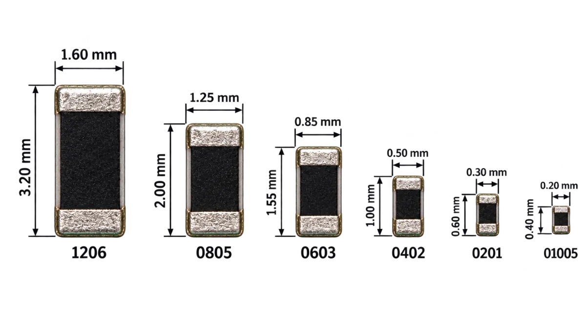
An SMD resistor is a fixed-value resistor in a leadless rectangular package that solders to pads on the surface of a printed circuit board rather than passing through holes. It is typically the most numerous component on a board, and the one most often specified from habit rather than from the datasheet. Most guides to…
Laminado revestido de cobre (CCL): tipos, fabricación, rendimiento y estándares
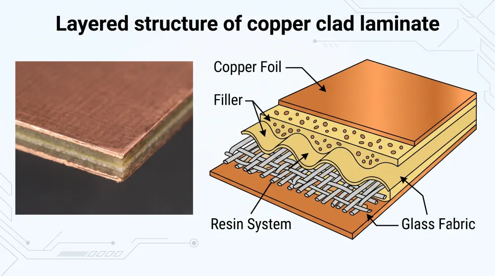
Copper clad laminate, or CCL, is a base material from which PCB conductors are formed. It consists of copper foil bonded to an insulating material such as cured glass-reinforced epoxy, a flexible polymer film, or a thermally conductive dielectric on a metal base. In a conventional multilayer rigid PCB, patterned CCL commonly becomes a core.…
JLCPCB vs. PCBWay: ¿qué fabricante de PCB se adapta a tu proyecto? (2026)
For a straightforward PCB prototype or a small assembly order that fits JLCPCB’s Economic PCBA rules, start with JLCPCB, especially when the components are already in its inventory. For rigid-flex or extensive custom fabrication requirements, shortlist PCBWay early. These recommendations follow from JLCPCB’s economical assembly tier and PCBWay’s documented advanced manufacturing options. The JLCPCB vs…

¿Qué es GND? Se explica el significado, los tipos y la conexión a tierra de PCB
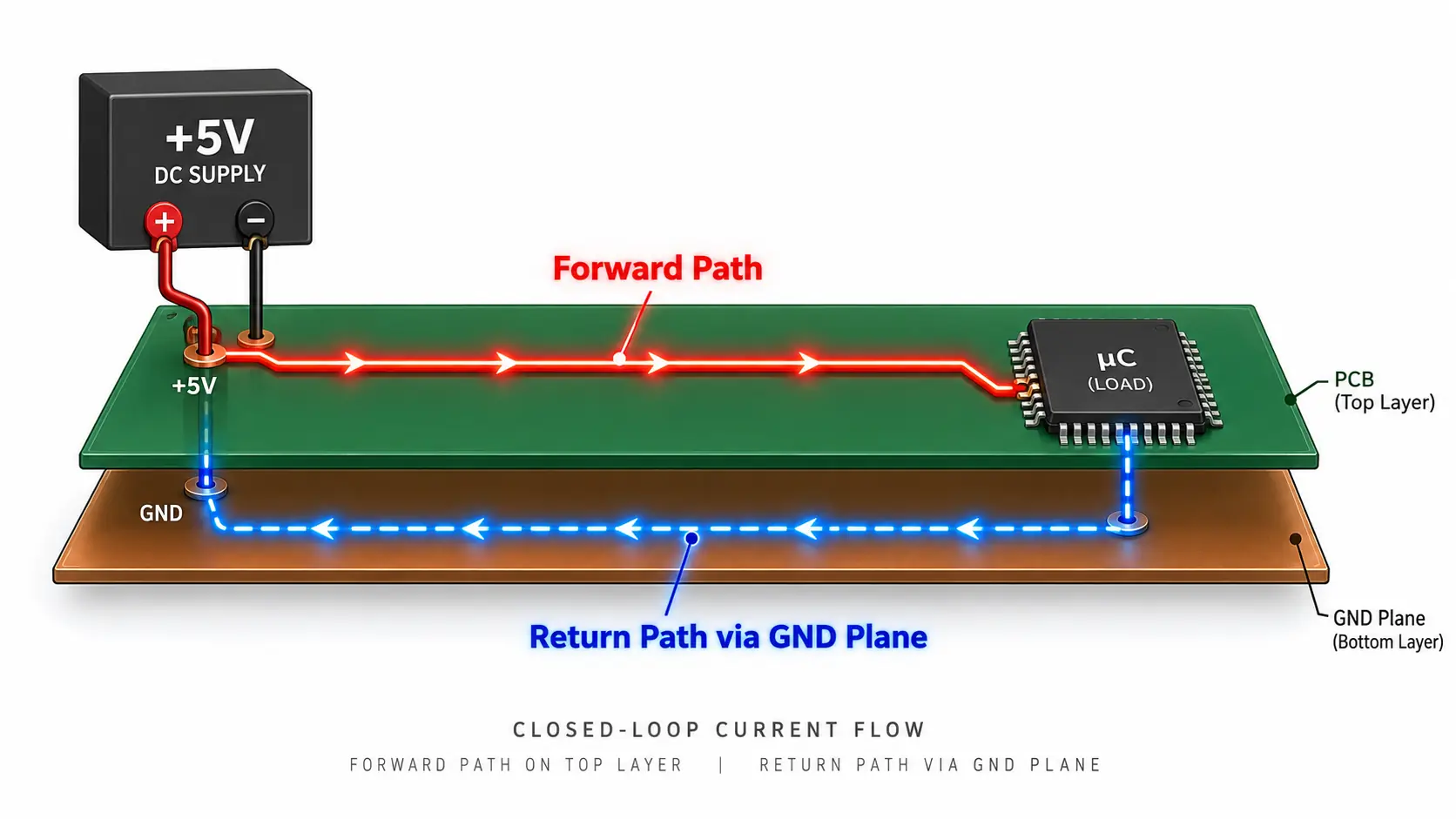
GND appears on almost every circuit diagram, PCB, power supply, and electronic module. It is often described as “zero volts” or “the negative terminal,” but neither description is universally correct. In electronics, GND stands for ground. It is the reference node against which other voltages are measured and, in many circuits, part of the path…
¿Qué es un agujero pasante? Tipos, usos y guía de diseño de PCB
A through hole is an opening that passes completely from one side of a printed circuit board (PCB) to the other. It may be plated with conductive copper to create an electrical connection, or left unplated for mechanical use. Through holes are commonly used for component leads, connectors, vias, mounting hardware, alignment pins, and slots.…

¿Qué son los paquetes QFN? Una guía práctica para el diseño y montaje de PCB
Los encapsulados QFN aparecen en todo, desde fuentes de alimentación y módulos inalámbricos hasta sensores, microcontroladores y electrónica automotriz. Su pequeña huella, caminos eléctricos cortos y transferencia de calor eficiente los convierten en una alternativa atractiva a los encapsulados con pines más grandes. Sin embargo, las mismas conexiones inferiores que ahorran espacio también hacen que el diseño de la huella del QFN, la soldadura y la inspección sean menos tolerantes. Entonces,…

Guía de material de PCB: tipos, propiedades y selección
El material de PCB afecta mucho más que la resistencia física de una placa de circuito. Influye en la impedancia, la pérdida de señal, la disipación de calor, la estabilidad dimensional, la fiabilidad del ensamblaje, la fabricabilidad, el plazo de entrega y el costo. Un material que funciona bien para un controlador básico puede fallar en un módulo de radar de 77 GHz, una placa LED de alta corriente o un dispositivo médico rígido-flexible.…

Diseño de PCB de impedancia controlada: apilado, especificaciones y pruebas
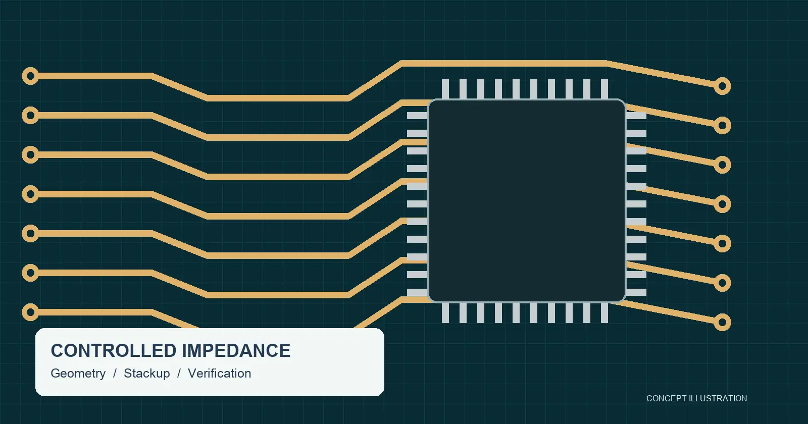
Controlled impedance is the practice of designing and manufacturing PCB traces so their characteristic impedance meets a specified target and tolerance. The result depends on the conductor geometry, dielectric construction, and reference planes. A complete requirement also states how the manufacturer will verify the finished structure. A note that says only “50 ohms” leaves important…
Resistencia de 10k: Código de colores, usos y cómo elegir la correcta
Una resistencia de 10k es un componente eléctrico pasivo con una resistencia nominal de 10,000 ohmios (10kΩ). En el diseño de circuitos moderno, es uno de los valores más ubicuos que se encuentran tanto en placas de pruebas como en PCB de producción. Ingenieros y aficionados recurren a las resistencias de 10k porque alcanzan un punto medio eléctrico ideal: limitan la corriente a niveles seguros,…

Diseño de antenas de PCB: distribución, materiales y fabricación
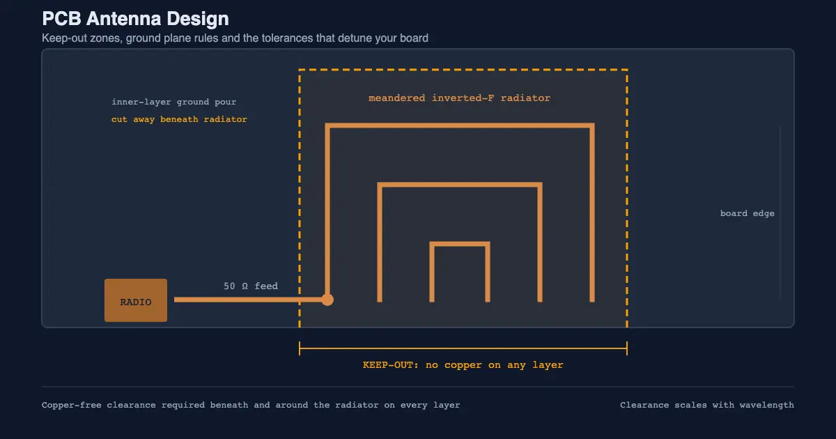
A PCB antenna is a copper trace or pattern etched directly onto a printed circuit board that transmits and receives radio frequency electromagnetic waves. It is the cheapest way to give a product wireless connectivity, because it adds no connector, no cable and no bill-of-materials line. It is also the part of a design most…
Ánodo y Cátodo de LED: Cómo Identificar los Terminales Positivo y Negativo
Un LED (diodo emisor de luz) es un dispositivo semiconductor polarizado que permite que la corriente fluya en una sola dirección. Para iluminar un LED, debes conectar correctamente sus terminales positivo y negativo dentro de tu circuito. En los LED estándar de orificio pasante, la pata más larga y el lado redondeado representan el ánodo, mientras que la pata más corta y el…