Blog
Hier können Sie Fachwissen erwerben, das die gesamte Kette vom PCB-Design bis zur Montage abdeckt, sowie präzise Analysen der neuesten Trends in der Elektronikindustrie.
Industrial PCB Production: Process & QA
Industrial PCB production turns an approved circuit-board design into bare boards and, when ordered, populated assemblies for industrial equipment. The route includes fabrication, component assembly, inspection and agreed testing. Approval depends on the specified build, operating conditions and acceptance criteria. A motor controller, sensor interface and cabinet-mounted control board can require different materials, mechanical support…
Aluminium-Leiterplatte: Thermisches Design und Materialien
An aluminum PCB is a printed circuit board that combines copper circuitry, an electrically insulating thermal dielectric and an aluminum base. The dielectric carries heat toward the metal while separating the circuit electrically. This construction is useful for LED lighting and power electronics when the board, mounting interface and cooling surface form a suitable heat…
HDI-Leiterplatte: Lagenaufbau, Mikrovias und Design
An HDI PCB, or high-density interconnect printed circuit board, uses fine conductors and compact interlayer connections to fit more wiring into a given area. Laser-drilled microvias and thin buildup layers help connect dense component pads without using a full-thickness hole at every connection. The design question is whether those features solve a routing constraint worth…

Starre Leiterplatte: Materialien, Aufbau und Designentscheidungen
A rigid PCB, or rigid printed circuit board, supports components and connects them through copper conductors on a substrate designed to retain its shape in service. It suits electronics whose circuitry stays fixed within an enclosure, rather than bending during use. Choosing one means matching its construction to the circuit, mounting, connectors and environment. Layer…

Flexible Leiterplatte: Typen, Materialien, Lagenaufbau und Designregeln
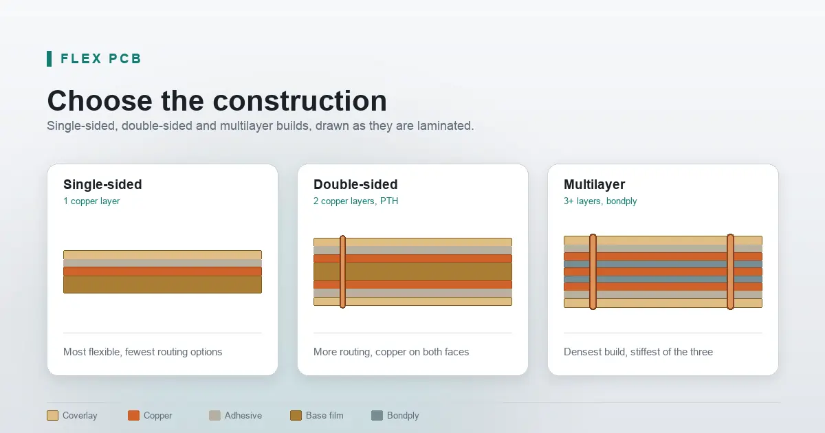
A flex PCB is a circuit built on a flexible polymer film, usually polyimide, with copper conductors bonded to it and a coverlay protecting them. That is the definition, and it is the part already answered above the search results. It is not the part that decides whether your build works. Four questions decide that,…
Biegeradius flexibler Leiterplatten: So wird er berechnet und spezifiziert
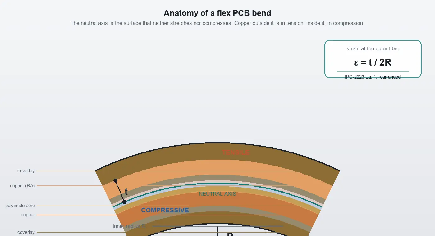
You have a stackup, a housing envelope, and a mechanical engineer asking for a flex PCB bend radius. The answer is not a lookup table; it is a strain calculation, and the multipliers in the tables are what that calculation returns once you fix a stackup. Every published multiplier, whether it reads 6×, 10×, 12×,…
Leitfaden zum Reflow-Löten: Prozess, Profil und Fehler
Reflow soldering is the process that attaches surface-mount components to a printed circuit board by heating stencilled solder paste until it melts, wets the component terminations and forms the joint on cooling. It is the primary assembly method for almost every modern electronic product, and it is the step where the most expensive mistakes become…
Was ist denn die stangenprüfung, sir? Messen, fehler und qualitätskontrolle
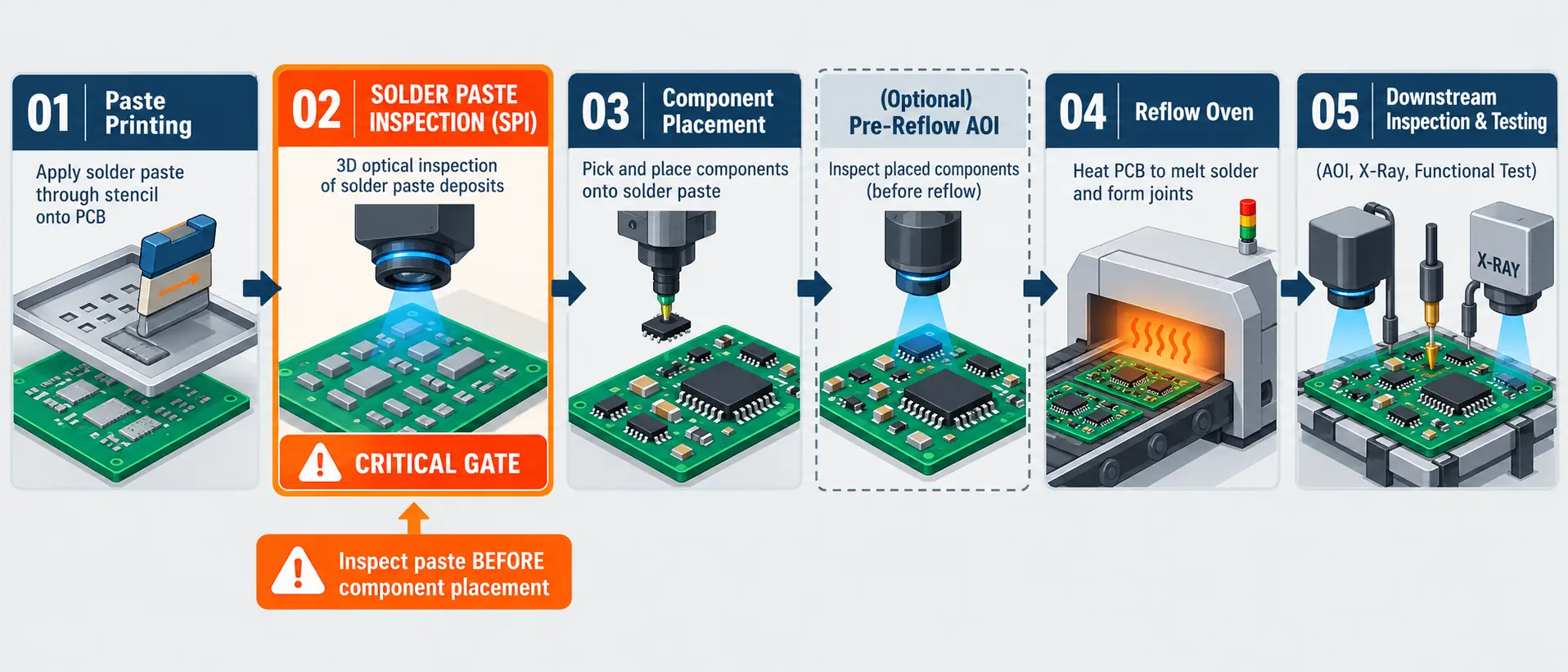
Solder paste inspection (SPI) checks paste deposited on a PCB after printing and before component placement. A 3D SPI system measures deposit volume, height, area, and alignment against programmed limits. It allows defective prints to be held and corrected before placement and reflow. For hardware engineers and PCBA buyers, the key decision is whether the…
Die 10 besten PCB-Design-Softwarelösungen im Jahr 2026
KiCad is the strongest free desktop starting point for engineers choosing PCB design software in 2026. Altium Designer through Altium Develop is a strong paid choice for small teams that want shared libraries, browser review, and electrical–mechanical collaboration in one connected workflow. Both support serious board design; the purchasing decision is whether the surrounding workflow…
Leitfaden zu SMD-Widerständen: Codes, Baugrößen, Footprints und Grenzwerte
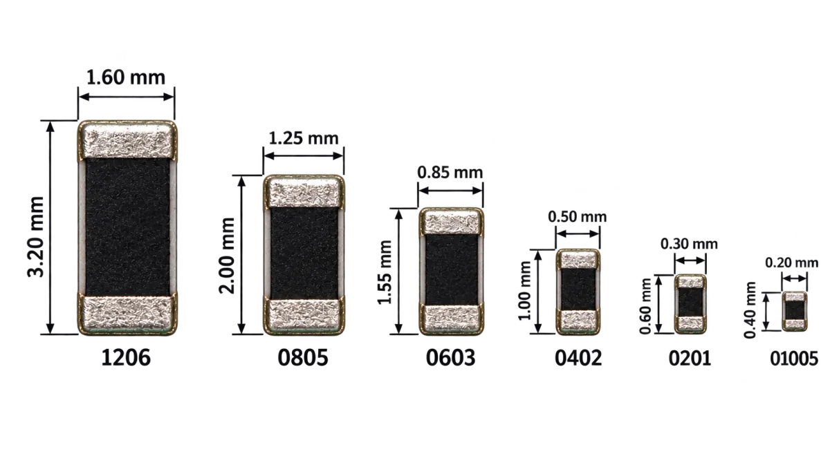
An SMD resistor is a fixed-value resistor in a leadless rectangular package that solders to pads on the surface of a printed circuit board rather than passing through holes. It is typically the most numerous component on a board, and the one most often specified from habit rather than from the datasheet. Most guides to…
Kupferkaschiertes Laminat (CCL): Typen, Herstellung, Leistungsmerkmale und Normen
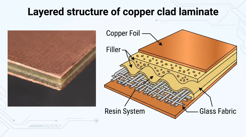
Copper clad laminate, or CCL, is a base material from which PCB conductors are formed. It consists of copper foil bonded to an insulating material such as cured glass-reinforced epoxy, a flexible polymer film, or a thermally conductive dielectric on a metal base. In a conventional multilayer rigid PCB, patterned CCL commonly becomes a core.…
JLCPCB vs. PCBWay: Welcher PCB-Hersteller passt zu Ihrem Projekt? (2026)
For a straightforward PCB prototype or a small assembly order that fits JLCPCB’s Economic PCBA rules, start with JLCPCB, especially when the components are already in its inventory. For rigid-flex or extensive custom fabrication requirements, shortlist PCBWay early. These recommendations follow from JLCPCB’s economical assembly tier and PCBWay’s documented advanced manufacturing options. The JLCPCB vs…

What Is GND? Meaning, Types, and PCB Grounding Explained
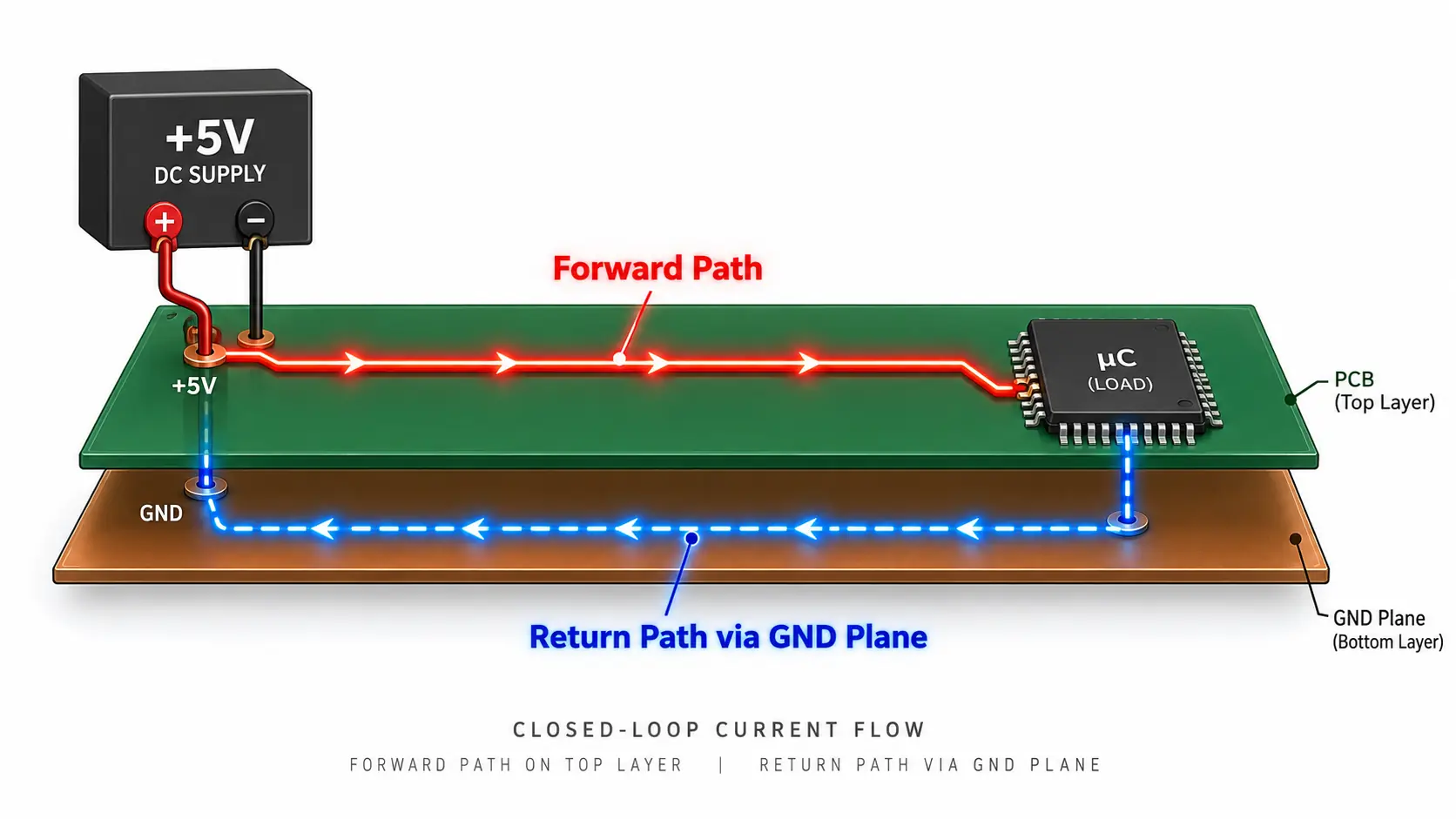
GND appears on almost every circuit diagram, PCB, power supply, and electronic module. It is often described as “zero volts” or “the negative terminal,” but neither description is universally correct. In electronics, GND stands for ground. It is the reference node against which other voltages are measured and, in many circuits, part of the path…
What Is a Through Hole? PCB Types, Uses, and Design Guide
A through hole is an opening that passes completely from one side of a printed circuit board (PCB) to the other. It may be plated with conductive copper to create an electrical connection, or left unplated for mechanical use. Through holes are commonly used for component leads, connectors, vias, mounting hardware, alignment pins, and slots.…

Was sind QFN-Gehäuse? Ein praktischer Leitfaden für PCB-Design und -Montage
QFN-Gehäuse finden sich in allem von Netzteilen und drahtlosen Modulen bis hin zu Sensoren, Mikrocontrollern und Automobilelektronik. Ihre geringe Grundfläche, kurzen elektrischen Pfade und effiziente Wärmeübertragung machen sie zu einer attraktiven Alternative zu größeren Gehäusen mit Anschlussbeinen. Allerdings machen dieselben Verbindungen auf der Unterseite, die Platz sparen, auch das Footprint-Design, Löten und die Inspektion von QFN weniger fehlerverzeihend. Also, …

PCB-Material-Leitfaden: Typen, Eigenschaften und Auswahl
Das PCB-Material beeinflusst weit mehr als nur die physische Festigkeit einer Leiterplatte. Es wirkt sich auf Impedanz, Signalverlust, Wärmeableitung, Dimensionsstabilität, Montagezuverlässigkeit, Fertigbarkeit, Lieferzeit und Kosten aus. Ein Material, das für eine einfache Steuerung gut geeignet ist, kann in einem 77-GHz-Radarmodul, einer Hochstrom-LED-Platine oder einem rigide-flexiblen medizinischen Gerät versagen.…

Leiterplatten-Design mit kontrollierter Impedanz: Stapeln, Spezifikationen und Tests
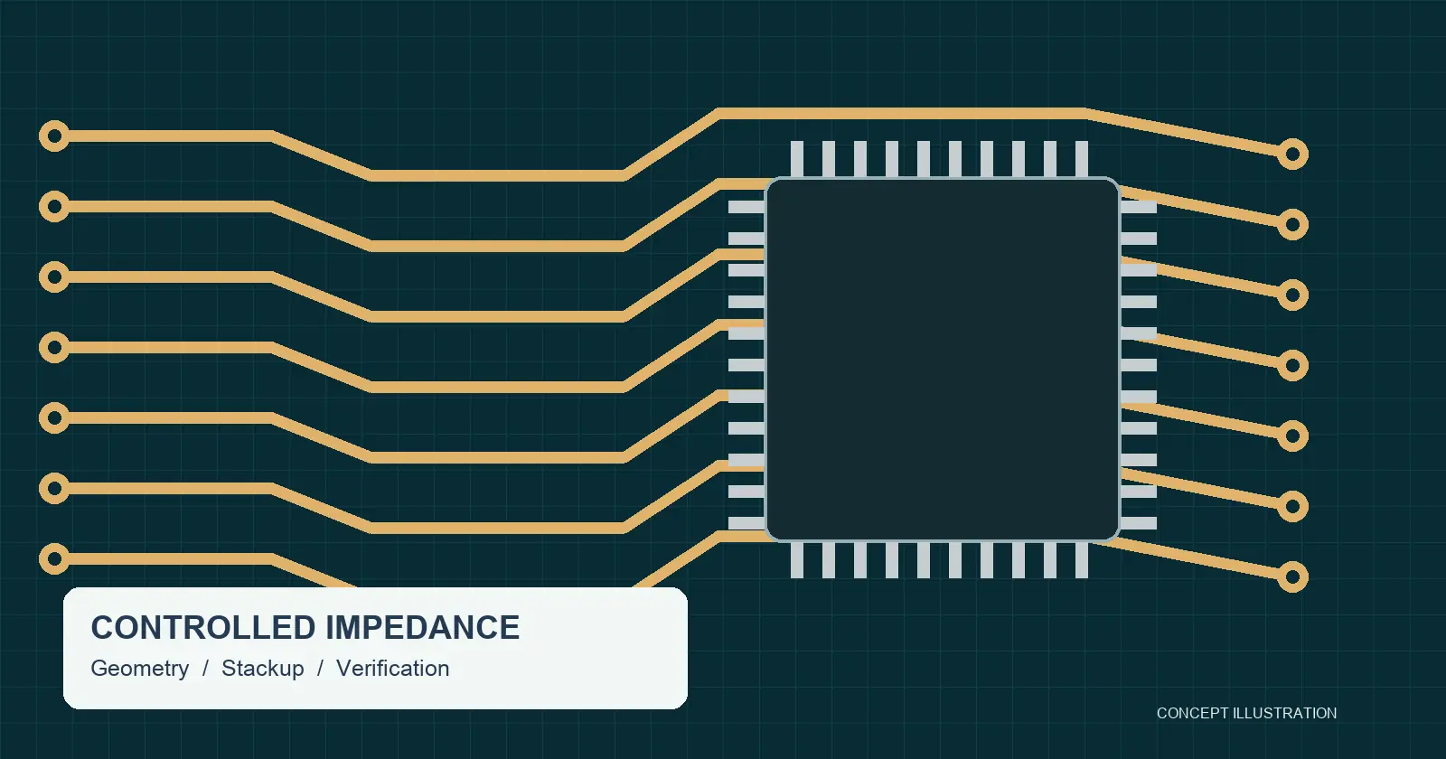
Controlled impedance is the practice of designing and manufacturing PCB traces so their characteristic impedance meets a specified target and tolerance. The result depends on the conductor geometry, dielectric construction, and reference planes. A complete requirement also states how the manufacturer will verify the finished structure. A note that says only “50 ohms” leaves important…
10k-Widerstand: Farbcode, Anwendungen und Auswahl des richtigen Modells
Ein 10k-Widerstand ist ein passives elektrisches Bauelement mit einem Nennwiderstand von 10.000 Ohm (10kΩ). Im modernen Schaltungsdesign ist er einer der am weitesten verbreiteten Werte, der sowohl auf Breadboards als auch auf Produktions-PCBs zu finden ist. Ingenieure und Hobbyisten greifen auf 10k-Widerstände zurück, da sie einen idealen elektrischen Mittelweg darstellen: Sie begrenzen den Strom auf sichere,…

PCB-Antennendesign: Layout, Materialien und Fertigung
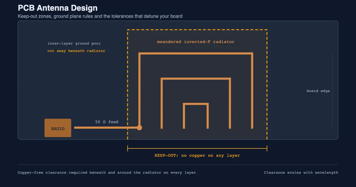
A PCB antenna is a copper trace or pattern etched directly onto a printed circuit board that transmits and receives radio frequency electromagnetic waves. It is the cheapest way to give a product wireless connectivity, because it adds no connector, no cable and no bill-of-materials line. It is also the part of a design most…
LED-Anode und -Kathode: So identifizieren Sie positive und negative Anschlüsse
Eine LED (Licht emittierende Diode) ist ein polarisiertes Halbleiterbauelement, das Strom nur in eine Richtung fließen lässt. Um eine LED zum Leuchten zu bringen, müssen Sie ihre positiven und negativen Anschlüsse in Ihrer Schaltung korrekt verbinden. Bei standardmäßigen Through-Hole-LEDs repräsentieren das längere Bein und die abgerundete Seite die Anode, während das kürzere Bein und die…