A rigid-flex PCB combines rigid circuit regions and flexible circuit layers in one construction. The rigid regions support components and can contain additional conductive layers, while the flexible region connects them through the enclosure. Conductors cross each rigid-to-flex transition to carry signals and power between regions.
次のような hypothetical compact device with a populated control region and a populated interface region on different sides of an internal enclosure corner. A flexible connection must route around that corner. For this example, the flex is bent during installation and remains stationary during normal operation; service handling still needs consideration. A rigid-flex design is one option alongside separate rigid boards with a cable and a flex circuit with local stiffeners.
要点
- Compare packaging, connections, assembly, service and validation before choosing rigid-flex over a cable or stiffened flex.
- Define the rigid and flex stackups together. A passive stiffener supports a flex circuit but does not add integrated rigid circuit layers.
- Route conductors through transitions, while placing the actual bend and stress-sensitive features away from those interfaces using fabricator-approved clearances.
- Specify how the assembly bends and is handled. Repeated movement calls for qualification under representative conditions, with agreed electrical pass/fail criteria.
- Compare the complete assembly cost and send the fabricator the regional construction, mechanical constraints and test requirements for a useful quote.
When does a rigid-flex PCB make sense?
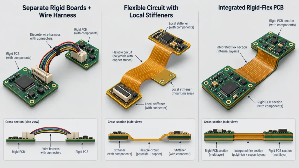
Rigid-flex is worth evaluating when connecting populated regions inside an enclosure creates a difficult packaging or assembly problem. For the hypothetical device, each of the three architectures changes where connections, assembly work and validation occur.
| Architecture | Packaging and connections | Service and verification |
|---|---|---|
| Rigid boards and cable | Boards link by cable; connectors need mating space. | Boards may be replaceable separately; check the cable path and contacts. |
| Stiffened flex | Continuous flex links supported component areas. | The circuit may need replacement as a unit; check joints and flex. |
| リジッドフレックス | Flex links rigid circuit regions; it can remove their cable and connectors. | The assembly may need replacement as a unit; check transitions and connections. |
Separate rigid boards can be designed independently, but the cable must be routed and mated during assembly. Replacing a board separately depends on connector access. Check connector retention and service access as well as the cable path and electrical contacts. The guide to rigid PCB construction covers the board side of this option.
Stiffened flex can connect locally supported component areas without an internal board-to-board cable. Passive stiffeners do not add electrically integrated rigid-board copper layers. Component assembly can require support fixtures; check enclosure fit, supported-area assembly, solder joints and flex behavior.
Rigid-flex integrates flexible circuitry with rigid regions that have their own conductive layers. The single assembly needs a coordinated stackup and manufacturing process. Check interlayer connections, transitions, mechanical fit and assembly access.
None of these choices wins for every device. A removable cable may be valuable for repair; integrated rigid-flex may be useful when the cable and mating space are difficult to accommodate. Cusack Electronics’ rigid-flex guide discusses construction and the distinction from stiffened flex. The broader guide to flex PCB types and design choices covers other flex configurations.
For the rest of the example, assume the team selects rigid-flex because the enclosure makes the internal cable and connectors awkward. That is a design hypothesis to check with a mechanical model, prototypes and supplier quotes, not a demonstrated saving.
How is a rigid-flex PCB stackup built?
A rigid-flex stackup defines which materials and conductive layers exist in each region and how they connect. A design might use a polyimide-based flexible circuit with copper conductors that continues into both rigid areas. The rigid areas can add glass-reinforced epoxy material such as FR-4 and further copper layers; plated connections in the rigid regions can connect those layers to the flex circuitry.
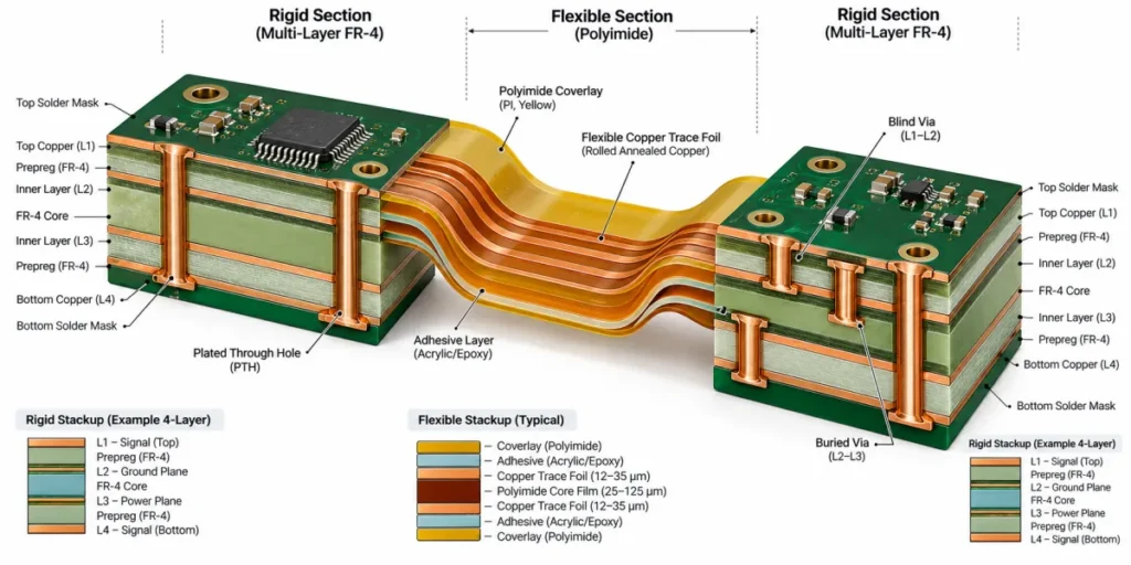
The exposed flexible span needs its own defined construction. A coverlay can protect copper on a flex surface, with openings where the design needs access; adhesives or bonding layers may also be part of the build. Layer order, materials and bonding choices depend on the design and fabricator. A rigid-to-flex transition is the interface where the rigid construction ends and the flexible span continues.
For the device, propose the flexible conductors needed between control and interface regions, identify the extra copper needed within each rigid region, and show where the relevant connections change layers. Ask the fabricator to review the complete regional stackup before treating it as buildable.
Design the transition and flexible region
Route through the rigid-to-flex transition
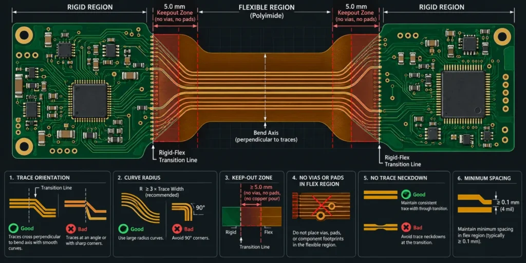
Traces must cross the transition to connect the rigid and flexible regions. Route them smoothly through the interface and avoid abrupt direction or width changes there. Where appropriate, route conductors across a bend approximately perpendicular to its axis; check the actual bend geometry and electrical routing needs before fixing the orientation.
Place pads, vias, plated holes and abrupt neckdowns away from transitions and active bend areas using clearances approved for the proposed construction. All Flex’s rigid-flex guidance recommends waiting until traces have exited the rigid area and cleared the keepout margin before necking them down, and advises against placing vias close to the boundary. Put the intended bend within the flexible span, away from the rigid interfaces, subject to the fabricator’s review. The clearance depends on the stackup and use, so a generic fixed keepout is not a substitute for an agreed drawing.
In the hypothetical enclosure, the conductors leave the control region, continue through the flex around the corner and enter the interface region. Show both transition boundaries and the intended bend on the drawing. Check that the available straight portions and enclosure clearance allow the bend to occur where planned, without pinching the flex or placing it against a sharp feature.
Define the bend and the motion
Mark the bend axis, the line about which the flex curves, as well as the bend location, direction and installed geometry. Check the design in three dimensions with the enclosure and assembly sequence. Include expected tolerances, any contact with the housing, and the path the flex takes while the product is opened or serviced.
この例では、通常の使用中、曲げた状態を保つことを想定しています。これは、使用中に繰り返し動くフレックスとは異なりますが、取り付けや修理の際には動きが加わることもあります。実際の動きに応じて、銅箔の選択、層構成、適合性、そして生じるひずみをすべて確認する必要があります。 Sierra Circuitsのフレックス設計ガイドライン では、配線と曲げに関する考慮事項を解説しています。曲げの計算や数値例については、別途用意されている フレックスPCBの曲げ半径ガイド.
材料と領域ごとの積層構成を指定する
標準的なリジッド基板の積層構成がアセンブリ全体に適用できると決めつけず、電気的要件と機械的要件の両方を確認できるだけの情報を基板メーカーに提供してください。
- 層構成: 各リジッド領域とフレックスに含まれる層、その順序、使用予定の材料、銅箔の仕様、カバーレイ、開口部、接着層を特定してください。領域の境界と、予定している層間接続も定義してください。
- 銅箔と動き: 想定する曲げ方を説明し、その用途に適した銅箔の種類、厚さ、加工方法、向きを基板メーカーに確認してください。適切な選択は、完成後の構造だけでなく、動き方にも左右されます。
- 電気的特性: 移行部をまたぐ信号経路とリターン経路を示してください。必要に応じて、該当領域のインピーダンス、間隔、電気的性能の目標値を指定し、積層構成の変化をどのように評価するか確認してください。
- 環境と組み立て: デバイスが耐える必要のある温度、湿気、化学物質などの条件に加え、関連する組み立て上および保守上の制約を明記してください。材料の選定については、 PCB材料ガイド.
この例では、提案するフレックスは、必要な制御部とインターフェース部の接続を確保しながら、角部に収まる必要があります。必要な配線によってフレックスの構造が変わる場合は、設計をリリースする前に、機械的な適合性と電気的性能の両方を再確認してください。
製造と組み立てが設計に与える影響
リジッドフレックスの製造では、リジッド領域とフレックス領域が意図どおりに位置合わせされ、接合される必要があります。 All Flexの製造概要 では、逐次積層、位置合わせ、樹脂の流動、カバーレイについて解説しています。実際の工程順序は提案される構造によって異なるため、早い段階で積層構成と図面を基板メーカーと確認してください。
サプライヤーがフレックス領域をどのように成形・保護し、位置合わせを維持してリジッド部とフレックス部の接合面を検査するのか確認してください。製造から組み立てまで回路を扱うために必要な、パネライズ、治工具、サポート方法についても相談してください。部品の配置やはんだ付け中にアセンブリを支えるため、キャリアや治具が必要になる場合があります。
小型デバイスでは、両方のリジッド領域で、部品、検査箇所、必要に応じて手直しする箇所にアクセスできるか確認してください。また、フレックスを筐体に無理に押し付けずに、作業者が回路を取り付けられるかも確認してください。折り曲げた後にどちらかの領域の検査や修理が難しくなる場合、組み立て計画だけでなく、アーキテクチャの選択にも影響する可能性があります。
リジッドフレックスPCBのコストを左右する要因は?
リジッドフレックスのコストは、その構造と、製造・検証に必要な作業によって決まります。領域ごとの層数、材料の選択、積層、位置合わせ、切り欠き、パネルの利用率、歩留まり、検査、発注数量は、いずれも見積もりに影響します。また、一体型の複雑な基板では、いずれかの領域に不具合があった場合の廃棄や交換のコストにも影響することがあります。
仮想デバイスについては、3つのアーキテクチャすべてで、同じ項目を比較してください。
- 基板単体と相互接続部品: 別体の基板、補強材付きフレックス、リジッドフレックスアセンブリの製造に加え、それぞれの設計で実際に必要となるケーブルやコネクターも比較してください。
- 組み立てと試験: 該当する場合はコネクターの嵌合、治具、取り扱い、検査、電気的または機械的な適格性評価を含めてください。
- 保守: アクセス性と、不具合のある領域を個別に交換できるか、それともより大きなアセンブリ全体を交換する必要があるかを考慮してください。
内部ケーブルとコネクターを取り除けば、見積もり対象となる部品や作業は変わりますが、リジッドフレックスが総組み立てコストで最も安くなるとは限りません。同じ数量、受け入れ基準、保守上の前提条件で比較できる見積もりを依頼してください。
量産前に設計を試験する
電気試験、機械的な適合性確認、フレックスの適格性評価では、それぞれ異なる点を確認します。試験結果を設計リリースの判断に使う前に、サンプル、方法、受け入れ基準について合意してください。
- 電気的な導通と絶縁: 試験するネットと、その導通および絶縁に関する受け入れ基準を定義してください。リジッド領域間の接続と、フレックスを横断する導体も含めてください。
- 構造と移行部の検査: 領域の境界、カバーレイ、関連する製造上の特徴をどのように検査するか合意してください。製造品について、追加の検査や代表的な断面観察が必要であれば、その内容も指定してください。
- 適合性と取り扱い: 代表的なアセンブリを筐体に取り付けてください。曲げ位置、接触箇所、部品へのアクセス性、およびデバイスで想定される組み立てと保守時の動きを確認してください。
- 該当する場合は、繰り返し曲げ: 実際の動作を定義し、代表的な回路または専用クーポンを用いて適格性を評価してください。曲げ形状、方向、動作速度、製品寿命中に想定される曲げ回数に基づくサイクル目標、環境、サンプル計画、電気測定を行うタイミングを含む電気的な合否基準について合意してください。試験対象の特徴を試験構造と配線が適切に再現していることを確認し、必要に応じて組み立て済み製品も別途確認してください。
この例のように静止状態で使用する場合は、適合性と取り扱いの確認が必要です。後の改訂でフレックスを動くヒンジに配置する場合は、その動きを再現した動的試験を追加してください。2025年10月の PCEA Flexpertsによるフレックス試験の解説 では、フレックス寿命の適格性評価はほぼ常に個別設計の試験であり、サイクル数は製品寿命中に想定される曲げ回数を超えるべきだと説明されています。ある時点で導通が確認されても、曲げ寿命が実証されたことにはなりません。また、クーポンの結果は、それが完成品の設計や使用状況をどの程度再現しているかを踏まえて解釈する必要があります。
IPCは、 IPC-6013F適格性評価・性能規格の改訂を発表しました。適用する規格、版、クラス、プロジェクト固有の受け入れ基準について、基板メーカーと合意してください。IPCに準拠しているというだけでは、回路がデバイス固有の動きに意図された期間耐えられることの証明にはなりません。用途に応じたフレックス寿命の適格性評価が必要です。
リジッドフレックスPCBメーカーに何を送ればよいですか?
組み立て品の平置き状態と取り付け状態を説明する製造用データ一式を送ってください。この仮想デバイスについては、制御部とインターフェース部を特定し、フレックスが両者の間をどのように通るかを示してください。以下を含めてください。
- 基板外形、レイヤー対応、ドリルデータ、領域境界、関連する寸法および公差を含む製造データと図面。
- リジッド部およびフレキシブル部の積層構成案、銅箔と材料の要件、カバーレイ開口部、表面処理、想定される層間接続。
- 曲げ軸、方向、位置、取り付け後に必要な形状を記載してください。動きが取り付け時、使用中、または繰り返し動作時に発生するかも明記してください。
- クリアランス、部品へのアクセス、役立つ機械モデルなど、筐体および組み立て上の制約。組み立てが対象範囲に含まれる場合は、組み立て情報も提示してください。
- 使用環境、および繰り返し動作がある場合は、その動き、目標サイクル数、認定条件。
- 試作および量産の数量、スケジュール、要求規格とその版、クラス、電気・検査・機械試験の合格基準。
最終リリース前に、提案された構造、製造能力、遷移部と曲げ部のクリアランス、試験方法、前提条件について製造業者に確認を依頼してください。見積もりを判断材料にする前に、平面図と取り付け後のモデルの相違を解消してください。
リジッドフレックスPCBに関するよくある質問
補強材付きフレックス基板はリジッドフレックスと同じですか?
いいえ。補強材はフレックス回路の一部を機械的に支えますが、それ自体が電気的に統合されたリジッドPCB層を追加するわけではありません。リジッドフレックスは、1つの構造内にフレキシブル回路とリジッド回路領域を組み合わせたものです。どちらも似たような実装上のニーズに対応できますが、実際の機器に必要な部品支持、組み立て、保守の要件に照らして比較してください。
リジッドフレックス回路は、繰り返し動作するように設計できますか?
はい。ただし、適性は構造と耐える必要のある動きによって異なります。使用時の形状と環境を指定したうえで、実際の使用を想定した動的試験、目標サイクル数、電気的な合否基準について合意してください。取り付け後に曲がった状態を保つ回路と、使用中に動き続ける回路では、用途の説明を変える必要があります。
小型機器の例では、次に、提案された領域別の積層構成と取り付け後の形状が、組み立て上の制約内で製造・検証できるかを判断します。要件がまとまったら、 リジッドフレックスPCB製造ページ から製造見積もりを依頼してください。