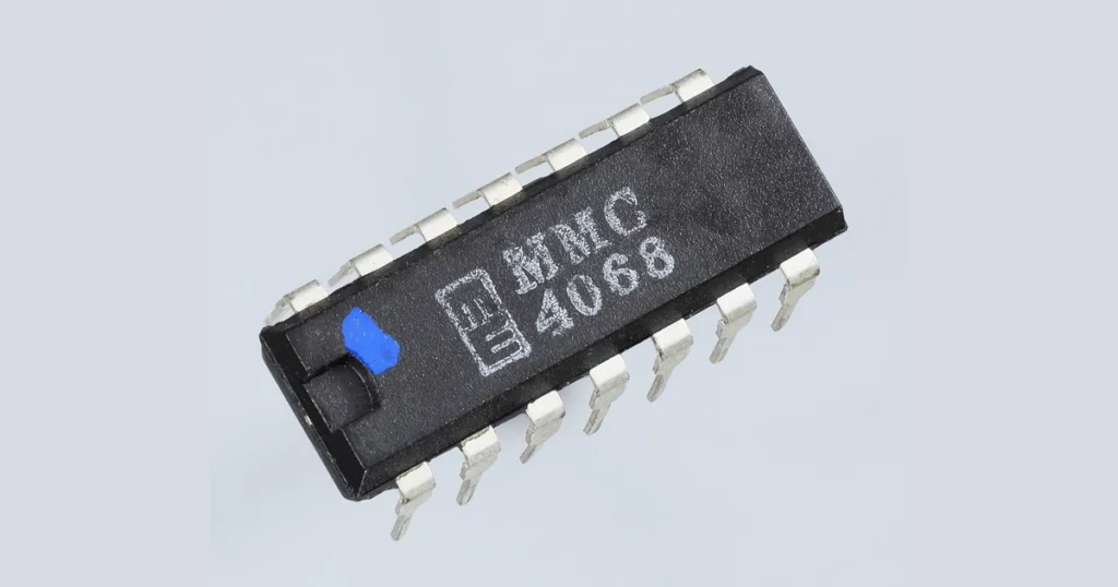
A dual inline package (DIP) is a component package with two parallel rows of leads. Many DIPs are inserted into holes in a circuit board or a socket. The package describes the part’s physical form; it does not tell you what the circuit inside does.
For a board designer, identifying a DIP is only the start. The exact part’s pinout, lead spacing and mechanical drawing determine the footprint. A socket introduces another set of dimensions to check.
要点
- Read the manufacturer’s pinout from the stated view and locate pin 1 before matching the part to a board.
- Pin pitch, distance between the two rows and package body width are different measurements. Check all three against the exact part.
- A socket is a mounting option. Matching the pin count alone does not prove that the component fits its contacts or that the socket fits the PCB.
- Agree on the finished-hole requirements, orientation markings and soldering process with the fabricator and assembler before production.
What Is a Dual Inline Package?
A dual inline package, also called a dual in-line package or DIL package, has leads arranged in two parallel rows along opposite sides of the body. Integrated circuits, switches and other components can use this arrangement. In the common through-hole form, the leads pass through PCB holes and are soldered, or they plug into a compatible socket.
DIP is a package description, not an electrical specification. Two eight-position DIPs can have different functions and pin assignments even when their outlines look similar. Through-hole components also come in many forms besides DIP; the broader through-hole PCB guide covers hole construction and fabrication.
How to Read a DIP Pinout
Start with the view specified in the datasheet. For the conventional eight-pin top view below, orient the notch toward the top. Pin 1 is at the upper left; numbering continues down the left side and then up the right side. Other packages can use different markings, so use the actual manufacturer’s diagram to confirm the starting point.
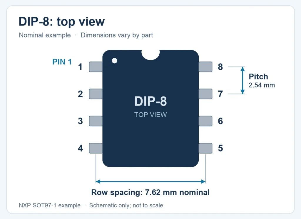
- Find the package view. A top view looks down at the marked face. A bottom or solder-side view reverses the apparent left and right positions.
- Find pin 1. The part drawing may show a dot, a notch or another index. Check the legend before treating a mark as the pin-1 indicator.
- Follow the numbering in the datasheet. On the eight-position example, pins 1–4 run down the left and pins 5–8 return up the right.
- Match the electrical functions. Read the pin table for the exact device; a number alone does not identify ground, supply or a signal.
- Compare the board and assembly drawing. Confirm that their pin-1 indicators match the component orientation, including the view used for each drawing.
For example, NXP’s ICM7555 data sheet, revision 2, shows pin 1 as ground and pin 8 as the supply for its DIP version. Those functions belong to that timer, not to every DIP-8.
DIP Package Dimensions: Pitch, Row Spacing and Body Size
The three dimensions most often confused are adjacent-pin pitch, row spacing and body width. They answer different questions:
| 寸法 | What it measures | 重要な理由 |
|---|---|---|
| Pin pitch | Center-to-center distance between adjacent positions in one row | Sets the spacing of holes along that row. |
| Row spacing | Center-to-center distance between the two rows | Sets the width of the nominal hole pattern. |
| Body width | Width of the molded or ceramic body | Helps establish component clearance and outline. |
| Lead size | Width, thickness or diameter of the lead at the relevant location | Affects hole fit or socket contact fit. |
| Lead length and height | Projection below the body and seated component height | Affect board thickness, soldering, clearance and enclosure fit. |
A pitch of 2.54 mm, or 0.1 inch, is common, but it is not universal. Nominal row spacings of 0.3 and 0.6 inch occur in DIP families; the number of pins does not determine which one applies. Reduced-pitch packages also exist. Use the part-specific drawing instead of choosing a footprint from the pin count alone.
NXP’s SOT97-1の外形図(2016年2月付)には、8ピンパッケージの公称ピッチが2.54 mm、公称列間寸法が7.62 mmと記載されています。ボディ幅寸法Eは6.20~6.48 mmです。また、この図面にはリードの全幅寸法M_Eとして7.80~8.25 mmが別途記載されています。これらの数値は異なる箇所を示すものです。ボディ幅やリードの自由端間隔を、公称の列パターンの代わりに用いないでください。
DIPの種類とソケット
DIPにはプラスチック製とセラミック製があります。プラスチック製DIPはPDIP、セラミック製はCDIPと略されることがあります。セラミック製の消去可能メモリ用パッケージには、ダイの上に窓が設けられているものもあります。パッケージの名称や寸法はメーカーによって異なるため、2つの部品が互換性を持つと判断する前に、注文コードと図面を確認してください。
ソケットは部品パッケージとは別のものです。ソケットのピンをPCBにはんだ付けし、ICをその接点に挿入します。これにより交換が容易になる場合がありますが、アセンブリの高さが増し、接点部分が追加されます。ソケットを選ぶ際は、ソケット固有の端子パターン、嵌合接点の寸法、クリアランス要件を確認してください。
ソケットの向きを示すマークにも注意が必要です。ソケット、IC、実装図それぞれにおけるメーカーの1番ピンの規定を確認してください。基板外形の切り欠きは、それが何を示すものかチームで確認した場合にのみ役立ちます。
PCB製造前にDIPのフットプリントを確認する方法
以下の例では、ある部品の図面をもとに、使用可能なソケットの検討から基板製造への情報引き継ぎまでを追います。これは文書に基づく説明であり、嵌合試験でも、部品購入の推奨でもありません。
1. 正確な部品とパッケージを特定する
NXPは、 ICM7555CN タイマーを8ピンのSOT97-1プラスチック製DIPとして掲載しています。NXPはこの部品を 生産終了としているため、これは過去の例です。新しい設計では、実際に選定する部品のライフサイクルと最新の資料を確認してください。
ICM7555のデータシートには、DIPのピン配置が示されています。図示された上面図では、1番ピンがグラウンド、8番ピンがVDDです。回路図シンボル、PCBのパッド番号、実装図でこれらの割り当てが維持されていることを確認してください。
2. 公称の穴パターンを作成する
SOT97-1の図面では、隣接するリード位置の間隔が2.54 mm、列間隔が7.62 mmと規定されています。各列には4つの位置があるため、列の最初から4番目の位置までの距離は、 列に沿って測ると ピッチ3つ分、つまり3 × 2.54 mm = 7.62 mmです。
この距離は、たまたまこの例の列間寸法と同じです。ただし、これらは別々の測定値です。別のパッケージでは、ピッチが同じでも列間隔が異なる場合があります。
ボディの外形だけでなく、リードの幅、厚さ、長さ、リード間隔も機械図面で確認してください。ライブラリの部品外形にはボディと周辺部品のための余裕を持たせ、可能な場合は配置後も1番ピンのマークが見えるようにしてください。 PCB DFMチェックリスト この資料では、製造前に行うべきその他の確認事項も取り上げています。
3. ソケットは別途評価する
OmronのXR2A-0801-Nは、列間ピッチが7.62 mmの8接点ソケットです。 DigiKeyが掲載しているXR2ソケットのデータシートには、ソケットのDIP端子用取付穴の直径が0.8 ± 0.05 mmとも記載されています。図面には底面図と記されています。穴寸法の指示がめっきや公差を経た後にどのように解釈されるか、製造業者に確認してください。この値は、ICリード用の普遍的な完成穴径ではありません。
列間ピッチが一致していても、 ではない このソケットとICが適合するとは限りません。NXPが示す例のリード寸法は、b1が0.38~0.53 mm、cが0.23~0.36 mmです。Omronは該当する平型リードの寸法を示し、対角寸法が0.56 mmを超える線材を使用しないよう注意しています。この資料からは、この線材に関する注意事項がこのICの平型リードに適用されるかどうかは分かりません。ソケットメーカーに適用の可否を問い合わせ、この組み合わせを指定する前に、適合性について文書による承認を得てください。
ICを基板に直接はんだ付けする場合は、ICのリード図面と基板製造業者および実装業者の要件に基づき、めっき後の完成穴径とパッドを選定してください。ソケットを使用する場合は、 ソケットの 端子に合わせて基板を設計し、ICとソケットの接点の適合性を別途確認してください。どちらの場合も、リード寸法、挿入クリアランス、製造公差、めっき、予定するはんだ付け工程を考慮してください。ドリル径がそのままめっき後の完成穴径になるとは限りません。
4. 決定事項を製造ファイルに反映する
| 確認項目 | この情報源を使用 | 誤っていた場合 |
|---|---|---|
| 部品番号とパッケージ | 部品表(BOM)と対象ICのデータシート | 異なるパッケージや回路の部品が供給される可能性があります。 |
| ピンの機能と1番ピン | ICのピン配置、回路図、実装図 | 部品の向きや接続を誤る可能性があります。 |
| ピッチ、列、ボディのクリアランス | ICまたはソケットの機械図面とPCBフットプリント | リードが穴に入らない、またはボディが干渉する可能性があります。 |
| 接点の適合性(ソケット使用時) | ICのリード寸法とソケットの接点仕様 | ピン数が一致していても、接続が適切とは限りません。 |
| 穴とパッドの要件 | 部品図面、基板製造業者、実装業者 | 挿入やはんだ付けが確実に行えない可能性があります。 |
| 向きと工程 | Assembly drawing, BOM and agreed build instructions | The assembler may lack the information needed to place or solder the part. |
Send consistent Gerber, BOM, placement and stackup information along with the relevant component and socket drawings. Identify the view of the board used in the assembly drawing and resolve any footprint or orientation question before fabrication.
DIP Assembly and Inspection
The right soldering method depends on the part, board, production volume and assembler. Through-hole leads may be soldered by hand, wave or a selective process. Some compatible parts can be assembled using pin-in-paste reflow alongside surface-mount components. Confirm the available process and its limits for the specific build.
- Check the parts and board. Compare markings and package codes with the BOM, and check the footprint and hole pattern against the approved drawings.
- Orient and insert. Match the manufacturer’s pin-1 mark to the assembly drawing. Seat the part or socket as required without forcing incompatible leads into the holes.
- Solder using an approved process. Protect temperature-sensitive parts and follow the component, solder-material and equipment guidance for the board. Qualify the process for the actual assembly.
- Inspect against the agreed criteria. Check orientation, seating and accessible solder joints. Agree on the applicable acceptance standard, revision and product class before deciding what is acceptable.
- Complete the agreed tests. Select electrical or functional tests for the project. Visual inspection alone cannot prove that the circuit operates correctly, and any inspection method has coverage limits.
For pin-in-paste, component temperature capability, standoff and placement must suit reflow. Paste volume and aperture design must also be adequate for the joint. AIM Solder’s pin-in-paste guide discusses these conditions and the trade-offs in depositing more paste.
A thermal qualification profile is not automatically a production recipe. Melexis’s through-hole soldering guidance distinguishes its device qualification conditions from the board-assembly profile developed for a particular process. Apply the limits for the actual component being assembled.
DIP vs Surface-Mount Packages
DIP and surface-mount device (SMD) describe different physical mounting arrangements. A surface-mount IC solders to pads on the board surface; a through-hole DIP uses leads that enter holes or a socket. The trade-off depends on the specific part and production process.
| 対価 | Through-hole DIP | Surface-mount IC |
|---|---|---|
| 基板上のスペース | Leads and holes can use more board area and constrain routing. | Many packages use less board area, although sizes vary. |
| 実装 | Requires insertion and a suitable through-hole soldering process. | Often placed and reflowed with other surface-mount parts. |
| Replacement | A compatible socket can make repeated replacement practical. | Replacement generally requires soldering equipment and access. |
| 検査 | Many leads and joints are visible, depending on the assembly. | Visibility depends on package geometry; some joints are hidden. |
| Part choice | Useful for some prototypes and legacy designs; availability varies. | Package and part choices depend on the device family. |
Changing the package does not guarantee an electrical drop-in replacement. Verify the pin functions, ratings, footprint and circuit requirements for both devices. For an example of surface-mount layout and inspection trade-offs, see the guide to QFN packages.
When Should You Choose a DIP?
A DIP can be useful when a compatible socket, breadboard or serviceable component supports the project. It may also be a practical choice when maintaining an existing board designed around that package.
Before selecting one for a new design, check the exact part’s availability, space around the footprint, routing constraints and assembly sequence. For compact or high-speed designs, evaluate lead and layout effects against the circuit requirements. A DIP is not automatically cheaper, stronger or easier to assemble for every application.
よくある質問
Are DIP and DIL the same?
Both abbreviations are used for dual in-line packages. Check the manufacturer’s drawing to identify the actual package dimensions and lead arrangement.
Does DIP-8 identify the circuit or its pin assignments?
No. DIP-8 describes an eight-position package, not the function of the component. Use the exact device’s data sheet for the pinout and electrical ratings.
Will any eight-pin DIP socket fit an eight-pin DIP?
No. Check row spacing and the shape, size and length of the IC leads against the socket contacts. Then check the socket’s own terminals and mounting-hole pattern against the PCB.
基板にはDIP部品と表面実装部品の両方を搭載できますか?
はい。混載基板では、スルーホール部品と表面実装部品を組み合わせられます。部品の耐熱温度や基板へのアクセス性を考慮し、実装業者と実装順序および工程を取り決めてください。
DIP実装の引き継ぎ準備
まず、正確な部品番号と最新のデータシートを確認してください。1番ピン、ピッチ、列間隔、リード形状、フットプリントを確認し、基板を発注する前にソケットと穴の要件を確定してください。プロジェクト固有のレビューをご希望の場合は、基板ファイル、BOM、部品およびソケットの図面、向きの詳細、実装要件を実装業者と共有してください。 PCB実装チームに.