You have a stackup, a housing envelope, and a mechanical engineer asking for a flex PCB bend radius. The answer is not a lookup table; it is a strain calculation, and the multipliers in the tables are what that calculation returns once you fix a stackup.
Every published multiplier, whether it reads 6×, 10×, 12×, 100× or 150×, comes from IPC-2223’s minimum bend radius equations evaluated at a chosen allowable copper strain. The circulating tables detached the number from the stackup that produced it, and that is why two engineers can both follow the standard and disagree by a factor of thirty.
This article puts the stackup back: the two equations, the three strain limits, the arithmetic that links them to the published multipliers, and how to put the result on a drawing.
flex PCB types, materials and design
핵심 요점
- A bend radius multiplier is not a rule. It is what you get when you fix a stackup, choose an allowable copper strain, and solve IPC-2223’s equations.
- The standard’s own dynamic worked examples give R/T of 31 for a 185 µm single-sided stack and 88 for a 320 µm double-sided stack, not the 100× and 150× that circulate in the field.
- IPC-2223 Figure 5-7 allows rolled annealed copper under 16% deformation and electrodeposited copper under 11%. That five-point gap is why dynamic flex requires RA foil.
- The 6× static rule is roughly an order of magnitude more conservative than the standard’s own installation-bend equation, which returns an R/T near 0.55 on a thin single-sided stack.
What Is a Bend Radius on a Flex PCB?
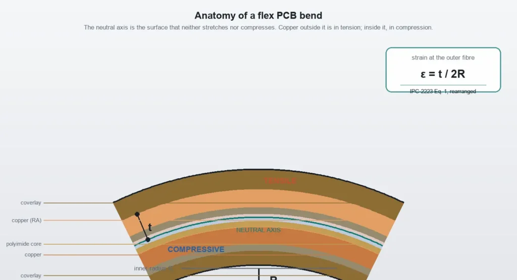
A flex PCB bend radius is the inner radius of the curved section: the distance from the innermost surface of the bent circuit to the centre of curvature.
That surface is where the calculation starts, not where the failure happens. Bend a flex circuit and the neutral axis sits somewhere inside the stack. Material outside the axis stretches; material inside it compresses. The outer foil is pulled toward its elongation limit while the inner foil buckles and delaminates from the coverlay adhesive.
The radius controls strain everywhere in the bend, and the mechanical envelope sets it. In one sentence: the radius scales with total flex thickness, scales with how far the outermost copper sits from the neutral axis, and on a fixed stack the dynamic multiplier lands close to two orders of magnitude above the static one. The standard’s own single-sided example gives R/T 31 against R/T 0.45.
How to Calculate the Minimum Bend Radius
IPC-2223 gives two equations, split by construction. Both work in micrometres.
IPC-2223 §5.2.3.4.1, single-sided with coverlay (Eq. 1):

    R = (c / 2) × [(100 - E_B) / E_B] - D

IPC-2223 §5.2.3.4.2, double-sided with coverlay (Eq. 2):

    R = (d / 2 + c) × [(100 - E_B) / E_B] - D

    R   = minimum bend radius, µm
    c   = copper thickness, µm
    d   = dielectric thickness in the flexible clad material, µm
    D   = dielectric thickness including adhesive, µm
    E_B = allowable copper deformation, %
These were read from the November 1998 base revision of IPC-2223. The current revision is IPC-2223F, dated May 2026, and the publisher’s current-revision listing is where to confirm which edition your fabricator builds to. Clause numbering has changed across revisions, so verify against a licensed copy. This article does not claim the text is identical in F.
D is subtracted because R is measured at the innermost surface, while D is the dielectric and adhesive between that surface and the copper. Thicker material under the copper puts the foil further out at the same inner radius, so a smaller R produces the same strain.
E_B takes three values: 16% for a single crease in rolled annealed copper, 10% for installation bending (flex-to-install, tied to the minimum elongation in IPC-MF-150), and 0.3% for repeated motion. Those three numbers are the only thing separating the multipliers.
Define T first. T is the sum of the base film, every copper foil, every adhesive or bondply layer, and the coverlay on both sides, measured in the bend region. It is not the nominal substrate thickness on the data sheet, and it is not the thickness at the stiffener, which is thicker by design and irrelevant to the bend. Two engineers disagreeing by a factor of two have almost always defined T differently.
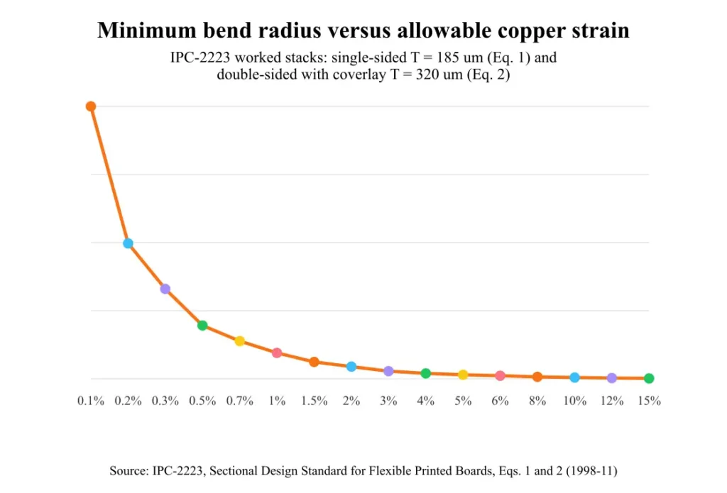
Take the standard’s single-sided example: 50 µm polyimide base, 25 µm adhesive, 35 µm copper, and coverlay with its adhesive. That is T = 185 µm, c = 35 µm, D = 75 µm. At E_B = 0.3%, Eq. 1 returns 5,741 µm, or 5.74 mm, an R/T of 31.
Take the double-sided example: a 50 µm polyimide core, two adhesive layers, two 35 µm copper foils, coverlay on both faces. That is T = 320 µm, d = 100 µm, c = 35 µm, D = 75 µm. At 0.3%, Eq. 2 returns 28,173 µm, or 28.17 mm, an R/T of 88.
Hold that stack fixed and change only the application. At the 10% installation limit, Eq. 1 returns 82.5 µm, or 0.083 mm, an R/T of 0.45. The geometry did not move; the answer moved by a factor of 69. A flex-to-install bend and a dynamic hinge are different design regimes.
That 0.083 mm is below anything you can form and inspect reliably, and the equation does not care. On a thinner stack the first term falls further, and D can exceed it, at which point Eq. 1 returns a negative radius. That is not an arithmetic error: it means the strain limit is no longer binding, because copper that thin tolerates almost any radius the process can produce. Read a negative result as “not the governing constraint” and set the drawing value from what the tooling and the coverlay will survive without creasing.
Report the diameter with the radius. A 5.74 mm radius is an 11.5 mm minimum bend diameter, and the mechanical engineer sizing the housing thinks in diameter, because that is the gap between two walls. Then add 20% to 30% for production: T varies with adhesive flow and lamination, and the formed radius carries its own tolerance. The 5.74 mm result becomes 6.9 mm to 7.5 mm.
Run the calculation on the finished stack, not the design intent. Coverlay adhesive flows during lamination, so the finished T sits a few micrometres above or below the nominal sum, and a fabricator quoting a build will give a finished thickness range rather than one number. Use the top of that range for a dynamic part. The radius scales linearly with T, so a 5% thickness overrun is a 5% radius overrun, and on a 28 mm dynamic radius that is well over a millimetre of housing nobody budgeted for.
Why the Multiplier Changes: The Strain Math
The equations are not empirical fits. They are the geometry of a bent beam written in the standard’s notation, and the rearrangement is short enough to do on a whiteboard. Bend a layer of thickness c so its inner surface has radius R. The neutral axis sits at R + c/2, the outer surface at R + c. The outer arc is longer in proportion to the radii, so strain at the outer fibre is (c/2)/(R + c/2), which reduces to c/(2R + c). Set that equal to E_B/100 and solve:
R = (c / 2) × [(100 / E_B) - 1]This is Eq. 1 with D removed. Add the dielectric offset back, because R is measured at the inner surface rather than at the copper’s inner fibre, and you have the standard’s equation exactly. The familiar relation epsilon = t/(2R), with t the distance from the neutral axis, is the same statement in approximate form: set t = c and invert, and you get (c/2)(100/E_B), which is the standard’s own expression without the small exact-form correction. The derivation belongs to IPC-2223. The point is that the equation is already the strain relation.
So a multiplier is the factor (100/E_B – 1) at a chosen strain, scaled by how far the copper sits from the axis and divided by total thickness. For the three limits that factor is 5.25, 9 and 332. Moving from 10% to 0.3% multiplies it by 37 before any geometric term changes.
The limits come from IPC-2223 Figure 5-7, which gives maximum deformation under 16% for rolled annealed copper and under 11% for electrodeposited copper. That gap answers the question designers ask most often about dynamic flex. RA foil is not preferred because of folklore about grain structure; the standard allows it roughly 45% more deformation before the copper is considered failed, and at 0.3% per cycle that margin separates a hinge that survives qualification from one that cracks.
Keep those base-foil figures separate from the plated-copper recommendations in §4.3.1.1 and §4.3.1.2, which give 12% and 18% elongation for electrolytically plated copper in through-holes, measured per IPC-TM-650 Method 2.4.18.1. They are different quantities on different features and they are not interchangeable with the RA and ED limits. A bend region contains base foil, not plated barrel, so Figure 5-7 is the figure that governs the radius.
One inconsistency is worth flagging rather than smoothing over. Figure 5-7 shows about 3% for installation bending, while the §5.2.3.4.1 worked calculation uses 10% for the same case. The two do not agree, and this article does not resolve which is intended. The 10% figure is the more permissive one, so a design built to 10% carries less margin than the number implies. Read 3% as conservative when the bend is formed once and must not crack in the field.
층수도 같은 지렛대 효과를 통해 영향을 줍니다. 층이 추가될 때마다 구리가 중립축에서 더 멀어지고 강성이 커지므로, 곡률 반경이 그대로이면 최외층 동박의 변형률이 높아집니다. 커버레이가 25 µm인 4층 적층판은 두께가 300 µm일 때 최외층 구리가 축에서 약 125 µm 떨어져 있습니다. E_B = 0.3%라면 R = 41.5 mm, 즉 R/T = 138이 필요합니다.
비대칭 접착제 기반 적층판에서는 중립축도 중앙면에 위치하지 않습니다. 접착제는 폴리이미드보다 부드럽고 구리 분포도 균일하지 않아 중립축이 더 단단한 쪽으로 이동합니다. 최외층 구리까지의 거리는 대칭 구조를 가정한 계산값보다 커지며, 실제 변형률도 구조가 시사하는 값보다 높습니다.
이제 현장에서 정적인 굽힘 규칙을 해석하는 방식을 바꾸는 결과를 살펴보겠습니다. 커버레이 25 µm, 접착제 12 µm, 구리 18 µm, 베이스 필름 25 µm로 이루어진 얇은 단면 적층판의 경우 T = 80 µm, c = 18 µm, D = 37 µm입니다. 설치 시 한계인 10%를 Eq. 1에 대입하면 R = 81 − 37 = 44 µm, 즉 R/T = 0.55입니다. 같은 두께 80 µm에 6× 규칙을 적용하면 480 µm가 됩니다. 이 곡률 반경에서 바깥쪽 구리에 발생하는 변형률은 허용치 10%의 약 5분의 1인 1.9%입니다. 정적 굽힘 배수는 표준의 최소값이 아니라 보수적인 경험칙입니다. 수작업 성형과 적층판 편차가 실제로 존재하므로 여유를 두는 것이 낭비는 아니지만, 그 여유를 선택한다는 점은 알아두어야 합니다.
제작 구조에 적용할 배수는 무엇인가
오른쪽 열의 값은 이 페이지에서 임의로 만든 범위가 아니라, 대표 적층 구조에 IPC-2223의 방정식을 적용해 얻은 R/T입니다.
| 상태 | 공표된 수치 | 방정식으로 얻는 값 | 적용 방법 |
|---|---|---|---|
| 정적, 단면 또는 양면, 설치 시 한 번 굽힘 | 6×~10× | 설치 시 한계인 10%에서 R/T 0.45~0.55 | 공표된 수치는 보수적입니다. 둘 다 적용 가능하며, 기본 안전값은 6×입니다. |
| 정적, 3층 이상 | 12×~24× | 적층 구조에 따라 달라지므로 계산해야 합니다. | 계산할 것 |
| 동적, 단층 | 100× | E_B 0.3%에서 R/T 31 | 185 µm 적층판에 대한 표준 자체의 결과와 100×는 거의 일치합니다. |
| 동적, 커버레이가 있는 양층 | 100×~150× | 표준의 320 µm 적층판에서 R/T 88 | 150×는 보수적이며, 얇은 적층판에는 100×도 타당합니다. |
| 동적, 3층 이상 | 100× 또는 “권장하지 않음” | 300 µm 4층 적층판에서 R/T 138 | 사용하지 마세요. 비접착 플라잉 리드 또는 경연성 전이 구조를 사용하세요. |
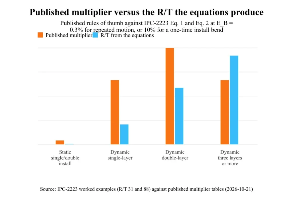
100×와 150×라는 수치가 아무 근거 없이 나온 것은 아니지만, 널리 알려진 것보다 적용 범위가 더 좁은 조건에서 나온 값입니다. 표준의 계산 예제에서는 변형률 0.3%일 때 두께 185 µm인 단면 적층판의 R/T가 31이고, 두께 320 µm인 양면 적층판의 R/T가 88입니다. 둥근 수치는 이 결과를 올림한 뒤 그 결과를 만들어낸 적층 구조와 분리한 것입니다. 100×는 단층 동적 굽힘 사례의 요약값으로, 150×는 양층 사례의 요약값으로 이해하세요. 구리가 2 oz이거나 적층판이 4층이어도 그대로 적용되는 규칙으로 받아들여서는 안 됩니다.
판단 기준:
- 설치 시 한 번 굽힘, 1~2층: 6×는 안전하고 10×는 더 안전합니다. 표준에서는 이보다 작은 값도 허용합니다. 손으로 굽힘을 만드는 경우에는 더 큰 값을 사용하세요.
- 한 번 굽힘, 3층 이상: 계산하세요. 두껍거나 비대칭인 적층판에서는 표의 정보만으로 판단하기 어렵습니다.
- 동적 굽힘, 구리층 1개: T의 100×를 적용하고, 0.3%에서 Eq. 1을 기준으로 확인한 뒤 필요한 반복 수명과 대조하세요.
- 동적 굽힘, 커버레이가 있는 양층: 150×를 적용하세요. 다만 적층판이 충분히 얇아 방정식에서 더 작은 값이 나오고 이를 뒷받침하는 시험 데이터가 있는 경우는 예외입니다.
- 동적 굽힘, 3층 이상: 굽힘 영역을 접착하지 마세요. 비접착 플라잉 리드를 사용하거나, 플렉스층을 1~2개만 사용하는 경연성 전이 구조를 적용하세요.
의존하기 전에 공표된 기준 두 가지를 바로잡아야 합니다.
Siemens의 경연성 기판 굽힘 설계 자료에서는 동적 플렉스의 곡률 반경이 플렉스 재료 두께의 최소 10배여야 한다고 설명합니다. 다른 모든 공표 자료는 최소 100×를 제시하며, 표준 자체의 두께 185 µm 적층판 동적 굽힘 예제는 R/T 31을 제시합니다. 10× 규칙은 표준 결과보다 한 자릿수 낮고 업계의 다른 기준보다 한두 자릿수 낮습니다. 이를 따르면 몇 차례 굽힘만으로 바깥쪽 동박에 균열이 생기는 힌지가 됩니다. 이 수치는 정적 굽힘이나 한 번 성형하는 조건을 동적 굽힘 규칙으로 제시한 것으로 보이며, 실제로도 그렇게 해석될 것입니다.
두 번째 수정 사항은 이 사이트와 관련이 있습니다. 이 사이트의 일반 플렉스 PCB 안내서는 동적 단층에 20×~40×, 동적 양층에 30×~50×를 제시합니다. 이는 공표된 합의 기준과 표준의 계산 예제보다 낮으며, 상당히 짧은 반복 수명도 허용할 때만 적용할 수 있습니다. 자체 적층 구조의 반복 굽힘 시험 데이터가 더 작은 곡률 반경을 뒷받침하지 않는 한 더 큰 값을 사용하세요. 이전 안내는 계산을 대신하는 선택지가 아니라 계산 결과에 의해 대체됩니다.
출처에서 언급하든 그렇지 않든 모든 배수에는 두 가지 조건이 따릅니다. 구리 종류가 RA인지 ED인지, 그리고 두께 수치에 무엇이 포함되는지입니다. 이 조건 없이 제시된 배수는 사양으로 볼 수 없습니다.
플렉스 전체 두께와 적층 구조
곡률 반경은 T에 비례하므로, 더 잘 휘는 재료를 찾기보다 적층 구조의 두께를 줄이는 것이 대개 더 작은 굽힘 반경을 얻는 가장 빠른 방법입니다.
| 층 | 정적 플렉스 | Dynamic flex |
|---|---|---|
| 동박 | 18 to 35 µm, RA or ED | 9 to 18 µm, RA only |
| Polyimide base film | 25 to 50 µm | 12.5 to 25 µm |
| Adhesive or bondply | Acrylic, 12 to 25 µm | Adhesiveless preferred; epoxy if bonding is required |
| 커버레이 | 25 to 50 µm per side | 25 µm per side with thin adhesive |
Standard foils are 9 µm (quarter ounce), 12 µm (third ounce), 18 µm (half ounce), 35 µm (one ounce) and 70 µm (two ounces). The 12 to 35 µm band is the production mainstream. Going to 9 µm buys a smaller radius and costs current capacity and handling robustness. Going to 70 µm for power in a bend region doubles the copper term against 35 µm, and the radius with it.
Copper type is not a preference in a dynamic build. Figure 5-7 allows RA under 16% and ED under 11%. At 0.3% per cycle you are far below both, but the gap governs how much process variation the part tolerates. Use RA for anything that moves repeatedly. For static flex, ED is acceptable and cheaper, and many fabricators default to it unless the drawing says otherwise.
Adhesive follows the same logic. Acrylic flows well and forgives lamination pressure; epoxy is stiffer and more dimensionally stable. For dynamic work the better answer is usually to remove it. An adhesiveless construction bonds copper directly to a cast polyimide film, eliminating a layer that creeps under cyclic load and cutting thickness at the same time. IPC-4204C is the material specification for the flexible metal-clad dielectrics these constructions use.
Do that trade explicitly. At a 100× multiplier, 25 µm of adhesive is 2.5 mm of radius and 5 mm of bend diameter. A designer who needs 5 mm of diameter back can often find it by deleting an adhesive layer rather than by opening the enclosure.
Keep vias out of the bend. JLCPCB’s “Flexible PCB Bend Radius: Design Guide & Rules” recommends 1.0 mm of clearance from the bend zone for static flex and 1.5 mm for dynamic. A via is a hole through the neutral axis with a copper barrel in it, and the barrel has almost no compliance in the direction the bend is pulling.
flex PCB manufacturing capabilities]
Bend Length, Tangent Length and Transition Zones
There is no published numeric minimum for the straight tangent section before or after a bend in IPC-2223. The word “straight” does not appear in the standard in this context, and “Tangent Corners” is only a figure label, not a dimensioned requirement. Anyone quoting a tangent length as an IPC value is quoting a fabricator’s practice.
The fabricator rules that do exist are useful. Eurocircuits’ guide to designing flex-to-install PCBs gives bend-zone length as L = (2π × bend radius) × (bend angle / 360), the arc length of the bend. One 180° bend at 5 mm radius consumes 15.7 mm of bend zone. The length scales with the number of bends, and that sum is often larger than the space the mechanical team allocated.
JLCPCB puts components and stiffeners at least 2.5 mm from the start of the bending region, and GCA Flex terminates stiffeners at least 1.5 mm from the bend zone start. Both make sense: a stiffener is a step change in flexural rigidity, and a bend starting at a rigidity step concentrates strain there.
Coverlay openings follow a different kind of rule. IPC-2223 §5.2.3.3 states that the circuit shall not be flexed or formed in an area where there is a discontinuity in the covercoat. That is a prohibition, not a dimension. There is no millimetre figure attached because in the standard’s model the correct distance is zero: you do not bend there. The 0.5 to 1.0 mm figures circulating from fabricators are DFM margins around that prohibition, sized to keep the bend clear of the stress concentration at an opening’s edge. They are good practice. They are not standard values, and quoting them as such invites an argument you cannot win.
The layout rule that follows is to stagger the discontinuities. The stiffener edge, the coverlay edge and the copper transition should not sit on the same plane across the bend region, so no single cross-section carries all three rigidity changes. Zoned construction is the practical version: build the bend as plain flex with coverlay both sides and no stiffener, no plated hole and no copper pour, and let the stiffeners and connectors live at the ends.
rigid-flex transition zone design]
How to Specify Bend Radius on a Fabrication Drawing
Put the number in a dedicated bend-region note or a bend table, not in the general tolerance block. A general tolerance applies to a feature the fabricator measures; a bend radius governs how the part is stacked, formed and tested.
Say which side the copper is on. A bend puts one foil in tension and the other in compression, and in a double-sided stack the outer foil is the one that cracks. If the assembly can be flipped, the drawing should say so, because a bend direction that puts the less critical copper layer outside is free margin.
Express both radius and diameter, with a tolerance. A production recommendation, not a standard value: ±0.1 mm or ±10%, whichever is greater. The percentage covers larger radii where a fixed 0.1 mm is unrealistically tight; the absolute figure covers small radii where 10% is too coarse to inspect.
The number alone is not a specification. It needs its context: the total thickness T used in the calculation, the bend angle, the direction of bend relative to the copper layers, whether the bend is static or dynamic, the target cycle count for a dynamic part, and the copper type.
A callout you can copy:
BEND REGION - SEE DETAIL B
  Minimum bend radius: 7.5 mm (diameter 15.0 mm), ±0.1 mm / ±10%
  Calculated per IPC-2223 Eq. 2 at E_B = 0.3%
  Total flex thickness T = 320 um (see stackup table)
  Bend angle: 180 deg, copper on outside of bend
  Application: DYNAMIC - 100,000 cycles, verify per IPC-TM-650 2.4.3
  Copper: rolled annealed (RA), 35 um
  Keep vias and stiffeners >= 1.5 mm from bend zone boundary
flex PCB manufacturing capabilities]
How Bend Radius Is Verified
A specified radius is a claim about endurance, and endurance is demonstrated by test rather than by geometry. The method is IPC-TM-650 Method 2.4.3, “Flexural Endurance, Flexible Printed Board Materials”, which determines the number of flexes to conductor failure. It originates with the Flexible Circuits Test Methods Subcommittee (D-15).
Be careful with the failure criterion. The method as published counts flexes to conductor failure, meaning an electrical open. Several vendor pages attribute a “10% resistance increase” criterion to it. That is a common misattribution. If resistance-rise criteria apply on your programme, they come from the applicable specification or drawing.
The method does not fix the test conditions either. Bend radius, stroke, cycle rate and specimen geometry for a given part are set by the applicable specification and drawing. A page publishing a universal cycle count for “a flex PCB” is describing its own test.
IPC-6013, the qualification and performance specification for flexible and rigid-flexible printed boards, is where flex endurance qualification is required, with the cycle count and bend radius specified by the applicable use category and performance class in the contract or drawing. Vendor sources that publish a cycle-count table attributed to IPC-6013 contradict each other and none cites a clause, so this article does not reproduce one.
Finally, IPC-A-600 is an acceptability and inspection standard, not a design standard. It defines defects such as conductor cracking and delamination in the bend area, and an inspector can reject a part against it, but it prescribes no geometric minimums. Using IPC-A-600 to answer “what radius do I need” is a category error.
IPC-A-600 acceptance criteria]
자주 묻는 질문
What is the minimum bend radius for a flex PCB?
It is calculated from your stackup, not looked up. For a one-time installation bend, Eq. 1 at the 10% limit returns an R/T near 0.45 to 0.55 on a thin single-sided stack, so 6× is a safe practical figure. For repeated motion at 0.3%, the standard’s own worked examples give R/T 31 for a 185 µm single-layer stack and 88 for a 320 µm double-layer stack with coverlay.
What is the minimum bend radius for a double-sided flex PCB?
IPC-2223’s worked example for a 320 µm double-sided stack with coverlay gives R/T 88 for dynamic flex at 0.3% strain, which is 28.17 mm, and R/T 2.15 for a one-time installation bend at 10%, which is 0.69 mm. Both assume rolled annealed copper. With ED foil the allowable deformation drops from under 16% to under 11%, and the margin goes with it.
Can a multilayer flex PCB be used for dynamic bending?
굽힘부가 접착된 상태라면 불가능합니다. 두께 300 µm의 4층 적층 구조에서는 가장 바깥쪽 동박이 중립축에서 약 125 µm 떨어져 있습니다. 변형률을 0.3%로 제한하려면 굽힘 반경이 41.5 mm, 즉 R/T가 138이어야 합니다. 이는 대부분의 제품에 들어가지 않으며, 적층 구조를 충분히 얇게 만들어 맞추면 4층을 사용하는 이유가 사라집니다. 힌지를 가로질러 접착되지 않은 플라잉 리드를 배선하거나, 1~2개의 플렉스층을 갖춘 리지드-플렉스 전환부에 굽힘부를 배치하세요.
플렉스 PCB는 몇 번까지 굽힐 수 있나요?
굽힘 수명은 소재가 아니라 설계에 따라 달라지며, 표에 적힌 값을 인용하는 것이 아니라 시험을 통해 확인합니다. IPC-TM-650 방법 2.4.3은 도체가 파손될 때까지 플렉스의 굽힘 횟수를 측정하며, 시험 조건과 합격 횟수는 적용되는 사양서와 도면에 명시됩니다. 적층 구조, 반경, 시험 조건과 연계되지 않은 공개 굽힘 횟수는 설계 입력값으로 사용할 수 없습니다.
온도에 따라 굽힘 반경이 달라지나요?
네. 구리의 연신율과 접착제의 탄성률은 모두 작동 온도 범위에 따라 달라지므로, 20 °C에서 안전한 반경도 온도 범위의 상한에서는 여유가 줄어듭니다. 접착제를 사용하는 구조는 접착제가 연화되고 크리프가 발생하기 때문에 무접착 구조보다 온도에 더 민감합니다. 최악의 사용 온도를 기준으로 지정하세요. 전력 스테이지 근처에 있는 부품이라면 라벨에 표시된 주변 온도가 최악의 사용 온도와 다를 수 있습니다.
굽힘 반경과 굽힘 직경은 어떻게 다른가요?
반경은 곡률 중심에서 안쪽 표면까지의 거리이고, 직경은 굽힘부 전체를 가로질러 측정한 값으로 반경의 두 배입니다. 반경이 5 mm이면 직경은 10 mm입니다. 도면에 굽힘 반경인지 직경인지 밝히지 않은 채 굽힘 5 mm라고만 적으면 모호합니다. 두 값을 모두 지정하세요. 간격을 정하는 기계 설계자는 직경을 기준으로 생각하고, 설계 방정식에는 반경이 사용됩니다.
결론
설계 가이드의 배수는 적층 구조를 제외한 변형률 계산값입니다. 적층 구조를 다시 반영하세요. 굽힘부의 전체 두께 T를 합산하고, 적용 분야에 맞는 변형률 한계(어닐링 구리의 단일 접힘은 16%, 설치 시에는 10%, 반복 운동에는 0.3%)를 선택한 다음 식 1 또는 식 2를 적용합니다. 그런 다음 20~30%를 더하고, 반경과 직경을 함께 표시하세요. 도면에는 구리 종류, 굽힘 방향, 굽힘 횟수와 함께 두 값을 모두 기입하세요.
계산 결과가 설치 공간에 들어맞지 않는다면, 일반적으로 도면에 적힌 수치를 낮추는 것이 아니라 적층 구조를 얇게 하거나 굽힘부의 층수를 줄여 해결합니다.