ブログ
ここでは、PCB設計から組み立てまでの全工程に関する専門知識に加え、エレクトロニクス業界の最新動向を的確に分析する知識を身につけられます。
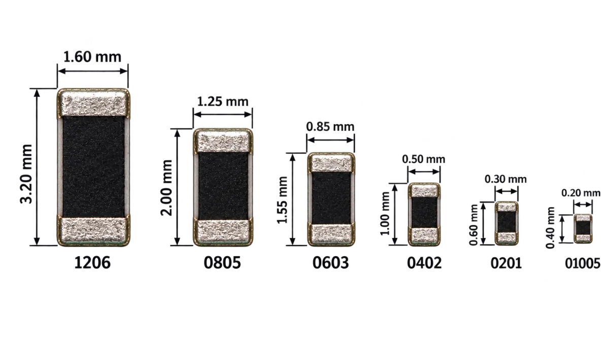
SMD抵抗器ガイド:コード、サイズ、フットプリント、定格
SMD抵抗器は、リードのない長方形のパッケージに収められた固定抵抗器で、プリント基板の穴に通すのではなく、基板表面のランドにはんだ付けします。一般に、基板上で最も数が多く、データシートではなく慣例に基づいて指定されることが最も多い部品です。多くのガイドでは…
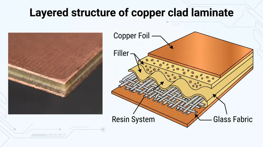
銅張積層板(CCL):種類、製造方法、性能、規格
銅張積層板(CCL)は、PCBの導体を形成するための基材です。銅箔を、硬化したガラス繊維強化エポキシ樹脂、フレキシブルなポリマーフィルム、または金属ベース上の熱伝導性誘電体などの絶縁材料に貼り合わせたものです。一般的な多層リジッドPCBでは、パターン加工されたCCLがコアになります。…
JLCPCBとPCBWayを比較:プロジェクトに合う基板メーカーは?(2026年)
For a straightforward PCB prototype or a small assembly order that fits JLCPCB’s Economic PCBA rules, start with JLCPCB, especially when the components are already in its inventory. For rigid-flex or extensive custom fabrication requirements, shortlist PCBWay early. These recommendations follow from JLCPCB’s economical assembly tier and PCBWay’s documented advanced manufacturing options. The JLCPCB vs…

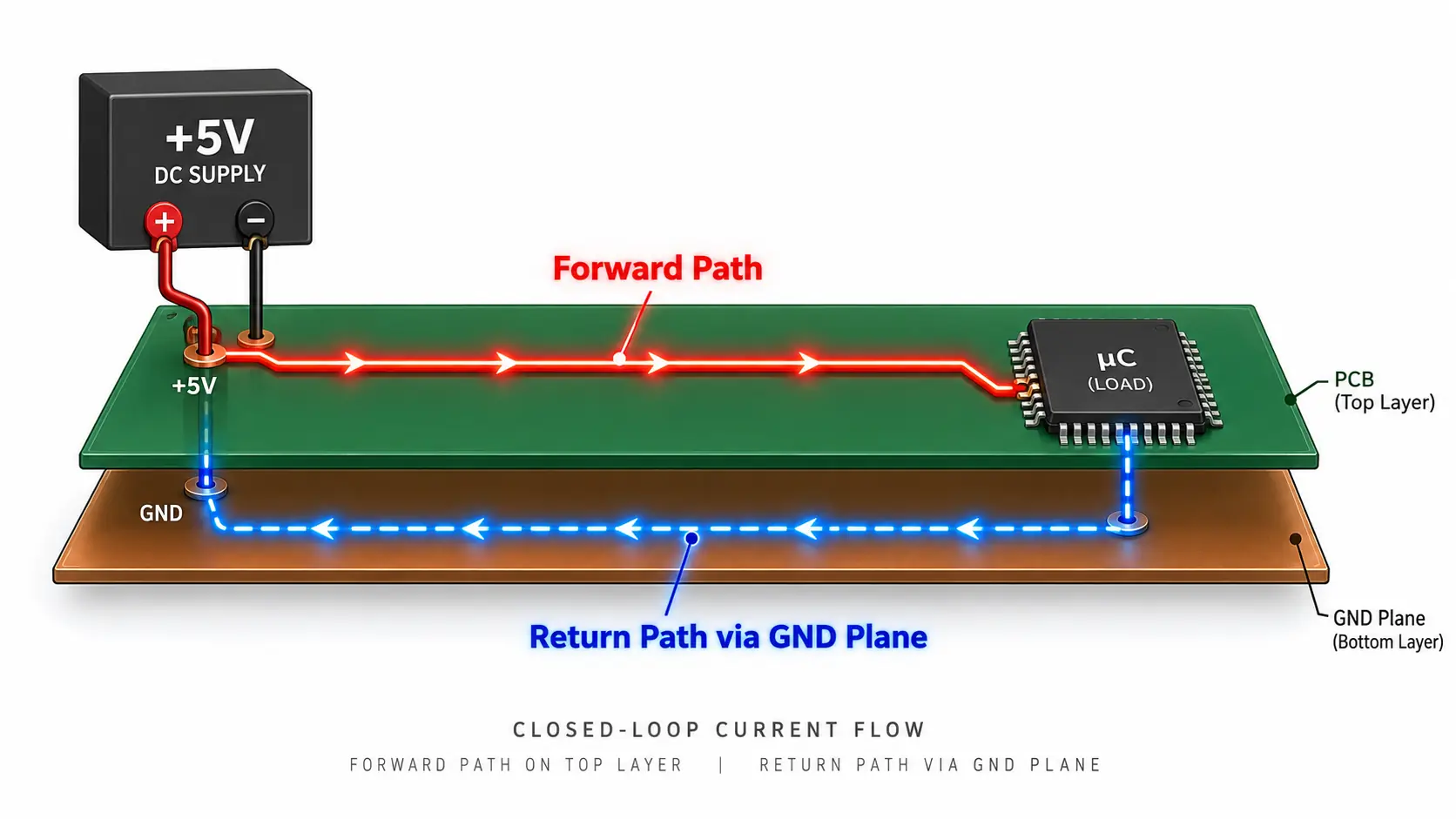
GNDとは?意味、種類、PCBのグラウンディングを解説
GND appears on almost every circuit diagram, PCB, power supply, and electronic module. It is often described as “zero volts” or “the negative terminal,” but neither description is universally correct. In electronics, GND stands for ground. It is the reference node against which other voltages are measured and, in many circuits, part of the path…
スルーホールとは?PCBの種類、用途、設計ガイド
A through hole is an opening that passes completely from one side of a printed circuit board (PCB) to the other. It may be plated with conductive copper to create an electrical connection, or left unplated for mechanical use. Through holes are commonly used for component leads, connectors, vias, mounting hardware, alignment pins, and slots.…

QFNパッケージとは?PCB設計・実装の実践ガイド
QFN packages appear in everything from power supplies and wireless modules to sensors, microcontrollers, and automotive electronics. Their small footprint, short electrical paths, and efficient heat transfer make them an attractive alternative to larger leaded packages. However, the same underside connections that save space also make QFN footprint design, soldering, and inspection less forgiving. So,…

PCB材料ガイド:種類、特性、選定方法
PCB material affects far more than the physical strength of a circuit board. It influences impedance, signal loss, heat dissipation, dimensional stability, assembly reliability, manufacturability, lead time, and cost. A material that works well for a basic controller may fail in a 77 GHz radar module, a high-current LED board, or a rigid-flex medical device.…

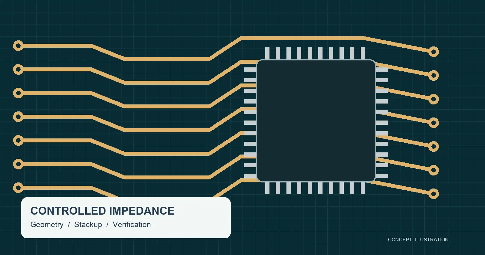
インピーダンス制御PCB設計:スタックアップ、仕様、試験
Controlled impedance is the practice of designing and manufacturing PCB traces so their characteristic impedance meets a specified target and tolerance. The result depends on the conductor geometry, dielectric construction, and reference planes. A complete requirement also states how the manufacturer will verify the finished structure. A note that says only “50 ohms” leaves important…
10kΩ抵抗器:カラーコード、用途、適切な選び方
A 10k resistor is a passive electrical component with a nominal resistance of 10,000 ohms (10kΩ). In modern circuit design, it is one of the most ubiquitous values found on breadboards and production PCBs alike. Engineers and hobbyists turn to 10k resistors because they hit an ideal electrical middle ground: they limit current to safe,…

PCBアンテナ設計:レイアウト、材料、製造
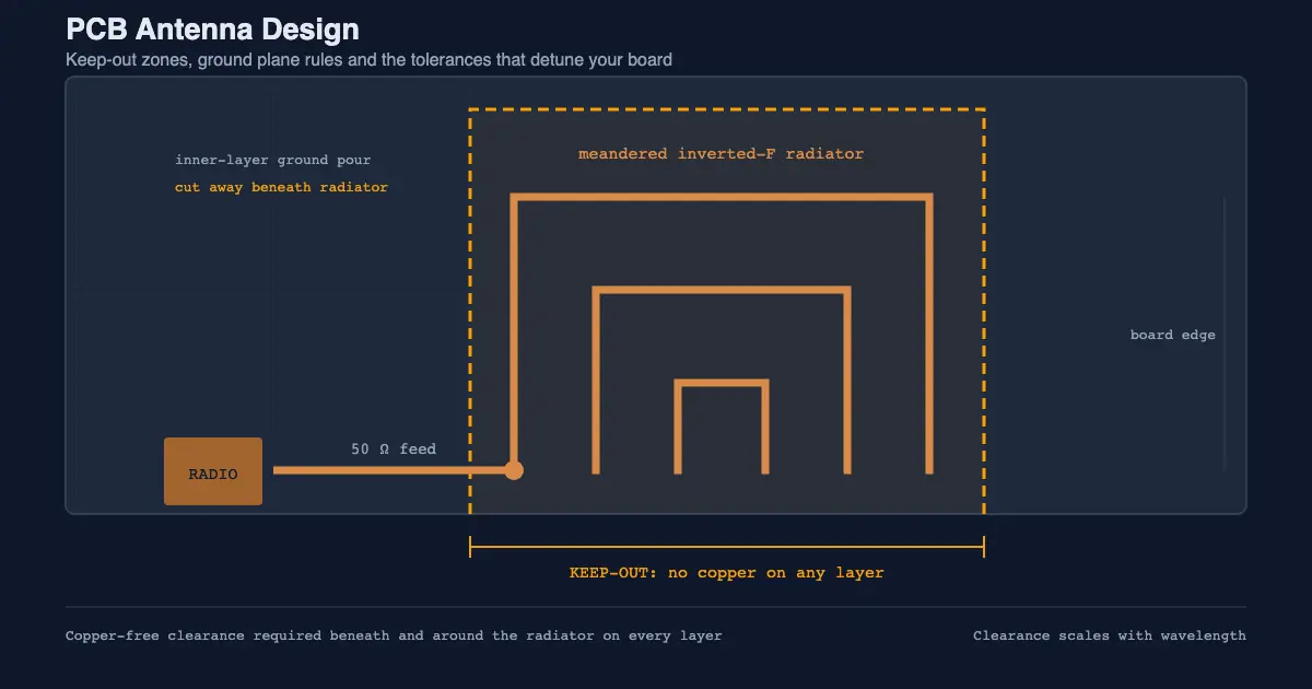
A PCB antenna is a copper trace or pattern etched directly onto a printed circuit board that transmits and receives radio frequency electromagnetic waves. It is the cheapest way to give a product wireless connectivity, because it adds no connector, no cable and no bill-of-materials line. It is also the part of a design most…
LEDのアノードとカソード:正極端子と負極端子の見分け方
An LED (Light Emitting Diode) is a polarized semiconductor device that allows current to flow in only one direction. To illuminate an LED, you must connect its positive and negative terminals correctly within your circuit. On standard through-hole LEDs, the longer leg and the rounded side represent the anode, while the shorter leg and the…

0402抵抗器ガイド:サイズ、仕様、選び方
Hardware design always comes down to a battle for board space. As consumer wearables, IoT devices, and high-performance computing modules pack more features into smaller enclosures, printed circuit board (PCB) real estate has become an incredibly valuable commodity. Moving away from legacy through-hole parts and bulkier surface-mount devices (SMDs) is no longer optional—it is a…
IPC-TM-650を解説:PCB試験方法、主要手順、品質管理での活用
“Test to IPC” is not a complete PCB requirement. A supplier still needs the method, revision, samples, conditions, and acceptance criteria before it can quote or run the work. IPC-TM-650 is the procedure side of PCB testing. It helps engineers choose a way to measure a board characteristic. The governing specification, drawing, or contract still…

PCB実装向けBOM:明確なPCBA用BOMの作成方法
A BOM for PCB assembly is more than a spreadsheet of parts. It is the sourcing and assembly control document that tells a PCBA manufacturer what to buy, what to populate, what to leave off, and which substitutions are allowed. If the BOM is unclear, the RFQ stalls before production ever starts. Many PCBA RFQ…
ガーバー、BOM、CPL、スタックアップ:各ファイルの意味
Gerber, BOM, CPL, and stackup files tell a PCB manufacturer four different things. Gerber files define the board layers. The BOM defines components. The CPL defines placement. The stackup defines layer construction, materials, copper, dielectric thickness, and impedance assumptions. Many PCBA quote delays happen before production starts. Why? The factory may have board data, but…

PCBAの見積もりにはどのファイルが必要ですか?
A PCBA quote needs more than Gerber files. For an accurate PCB assembly quotation, send Gerber files, drill files, BOM, CPL, stackup if needed, quantity, lead-time target, and test requirements. These files tell the manufacturer what to fabricate, what to source, where to place parts, and how the finished board should be accepted. If those…


PCBラミネート選定のためのFR-4材料特性
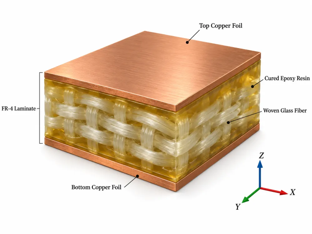
The FR-4 material properties that matter most depend on what your PCB must withstand: electrical signals, assembly heat, operating temperatures, voltage stress, moisture, and mechanical loading. Start with dielectric constant and loss, thermal expansion and stability, insulation performance, and mechanical requirements. FR-4 is a flame-retardant, glass-reinforced epoxy material class. It does not identify one fixed…
PCB熱ホットスポットマップ:シミュレーションと設計改善
A PCB thermal hotspot map helps engineers find where heat concentrates before it becomes drift, derating, solder fatigue, or field failure. Instead of treating thermal review as a late-stage check, the map turns temperature into layout evidence: which packages, copper areas, vias, planes, and airflow routes carry the thermal load. For PCB engineers, the value…