PCB 설계
여기에서 PCB 설계부터 조립까지 전 과정을 아우르는 전문 지식과 전자 산업의 최신 동향에 대한 정확한 분석을 얻을 수 있습니다.
2026년 최고의 AI PCB 설계 소프트웨어 도구 10선
최적의 AI PCB 설계 소프트웨어는 수행하려는 작업에 따라 다릅니다. 일부 도구는 요구 사항을 회로도와 자재 명세서(BOM)로 변환하는 데 도움을 줍니다. 다른 도구는 기존 설계의 부품 배치, 배선 또는 검증을 지원합니다. 생성된 레이아웃도 실제 적용 전에 엔지니어가 회로를 확인하고 준비해야 합니다.…
알루미늄 PCB: 열 설계 및 재료
알루미늄 PCB는 구리 회로, 전기 절연성을 갖춘 열전도 유전체, 알루미늄 베이스를 결합한 인쇄회로기판입니다. 유전체는 회로를 전기적으로 절연하면서 열을 금속 쪽으로 전달합니다. 기판과 장착 인터페이스, 냉각면이 적절한 열 경로를 형성할 때 이 구조는 LED 조명과 전력 전자 분야에 유용합니다.…
HDI PCB: 적층 구조, 마이크로비아 및 설계
HDI PCB(고밀도 상호 연결 인쇄회로기판)는 가는 도체와 소형 층간 연결부를 사용해 주어진 면적에 더 많은 배선을 배치합니다. 레이저로 가공한 마이크로비아와 얇은 빌드업층은 모든 연결부에 관통 구멍을 사용하지 않고도 조밀한 부품 패드를 서로 연결할 수 있게 합니다. 설계에서 고려할 점은 이러한 특징이 배선 제약을 해결할 만큼의 가치가 있는지입니다.…

플렉스 PCB 굽힘 반경: 계산 및 지정 방법
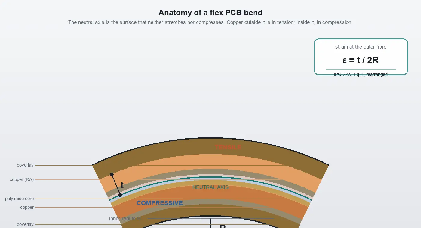
적층 구조와 하우징 공간이 정해졌고, 기구 설계 엔지니어가 플렉스 PCB의 굽힘 반경을 묻고 있습니다. 답은 단순한 표에서 찾을 수 있는 값이 아닙니다. 이는 변형률 계산의 결과이며, 표에 나온 배수는 적층 구조를 정한 뒤 계산으로 얻는 값입니다. 6×, 10×, 12× 등으로 표시되는 모든 공개 배수는…
2026년 최고의 PCB 설계 소프트웨어 10선
2026년에 PCB 설계 소프트웨어를 고르는 엔지니어에게 KiCad는 가장 강력한 무료 데스크톱 입문 도구입니다. Altium Develop을 통해 제공되는 Altium Designer는 공유 라이브러리, 브라우저 기반 검토, 전기·기계 분야 협업을 하나의 연결된 작업 흐름에서 원하는 소규모 팀에 적합한 유료 선택지입니다. 두 제품 모두 본격적인 기판 설계를 지원하며, 구매 결정의 핵심은 주변 작업 흐름입니다.…
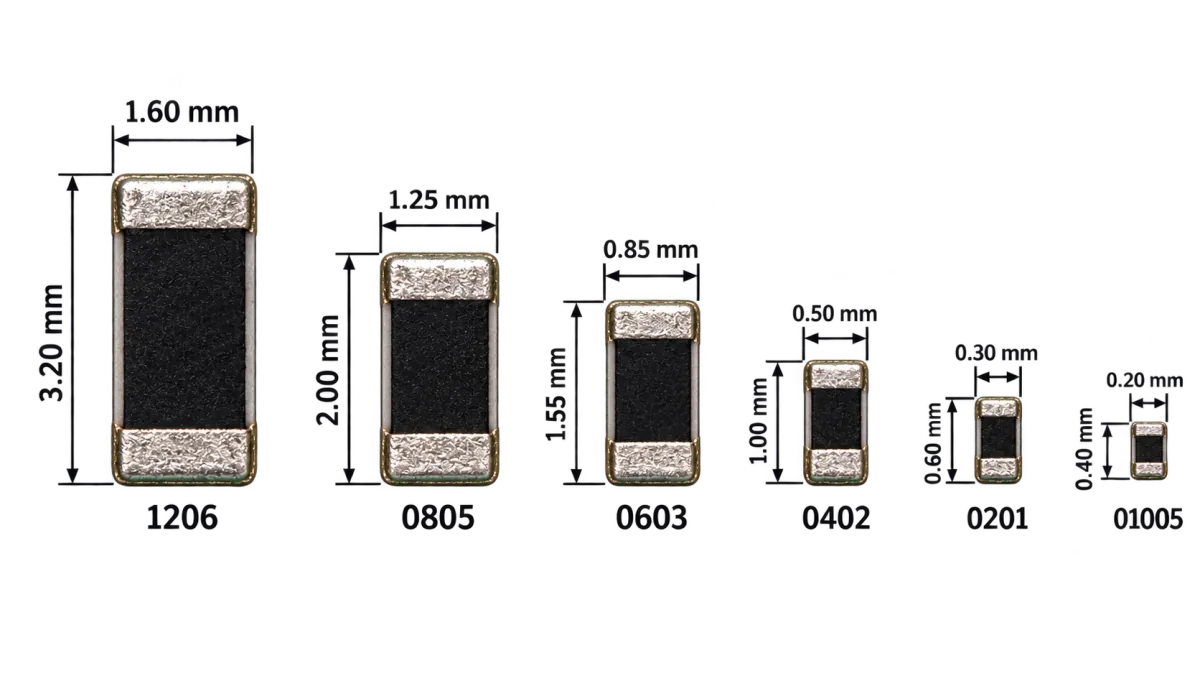
SMD 저항기 안내: 코드, 크기, 풋프린트 및 한계
SMD 저항기는 리드가 없는 직사각형 패키지의 고정값 저항기로, 구멍에 삽입하는 대신 인쇄회로기판 표면의 패드에 납땜됩니다. 일반적으로 기판에서 가장 수가 많은 부품이면서 데이터시트보다 관행에 따라 사양이 정해지는 경우가 가장 많은 부품이기도 합니다. 대부분의 안내 자료는…
QFN 패키지란 무엇인가요? PCB 설계 및 조립을 위한 실용 가이드
QFN packages appear in everything from power supplies and wireless modules to sensors, microcontrollers, and automotive electronics. Their small footprint, short electrical paths, and efficient heat transfer make them an attractive alternative to larger leaded packages. However, the same underside connections that save space also make QFN footprint design, soldering, and inspection less forgiving. So,…

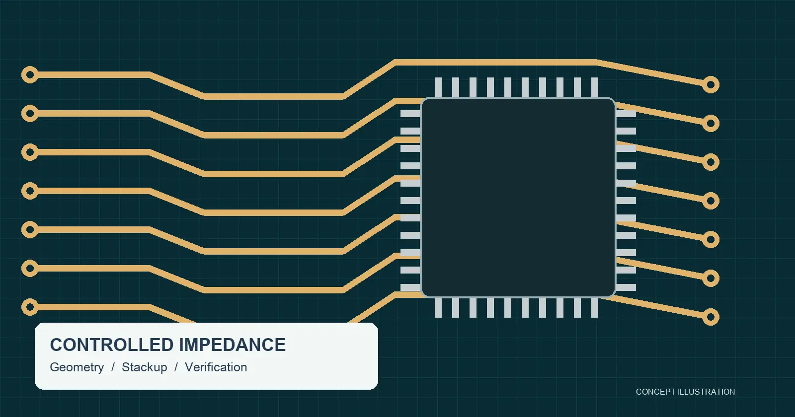
제어 임피던스 PCB 설계: 적층 구조, 사양 및 테스트
Controlled impedance is the practice of designing and manufacturing PCB traces so their characteristic impedance meets a specified target and tolerance. The result depends on the conductor geometry, dielectric construction, and reference planes. A complete requirement also states how the manufacturer will verify the finished structure. A note that says only “50 ohms” leaves important…
10k 저항기: 색상 코드, 용도 및 적합한 제품 선택 방법
A 10k resistor is a passive electrical component with a nominal resistance of 10,000 ohms (10kΩ). In modern circuit design, it is one of the most ubiquitous values found on breadboards and production PCBs alike. Engineers and hobbyists turn to 10k resistors because they hit an ideal electrical middle ground: they limit current to safe,…

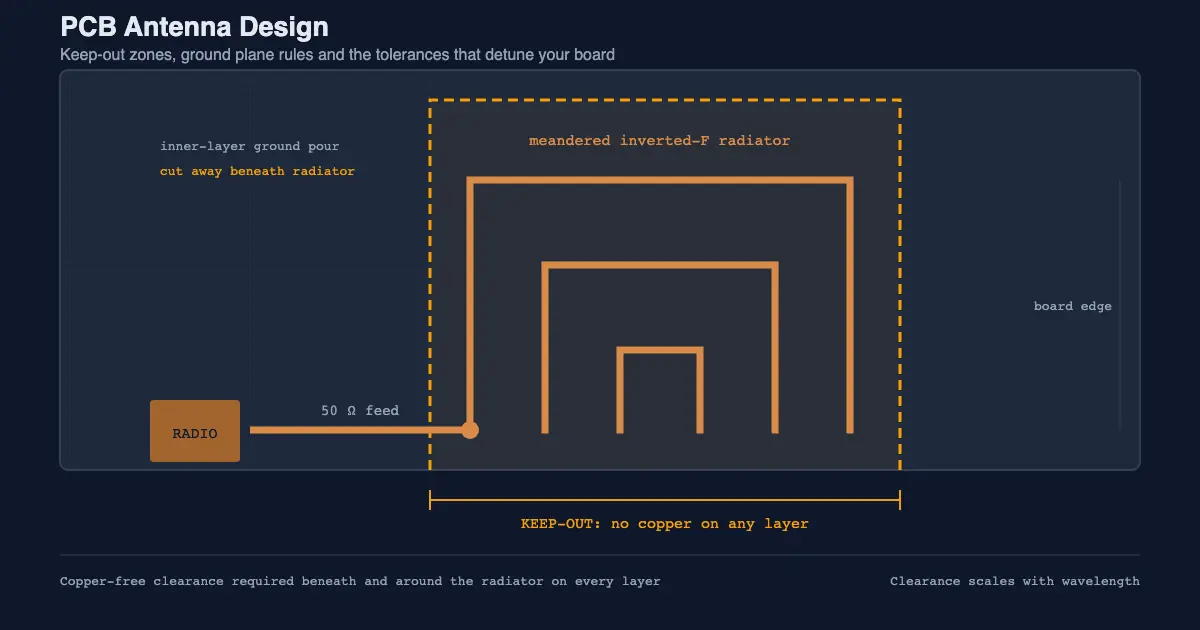
PCB 안테나 설계: 레이아웃, 재료 및 제조
A PCB antenna is a copper trace or pattern etched directly onto a printed circuit board that transmits and receives radio frequency electromagnetic waves. It is the cheapest way to give a product wireless connectivity, because it adds no connector, no cable and no bill-of-materials line. It is also the part of a design most…
PCB 라미네이트 선택을 위한 FR-4 재료 특성
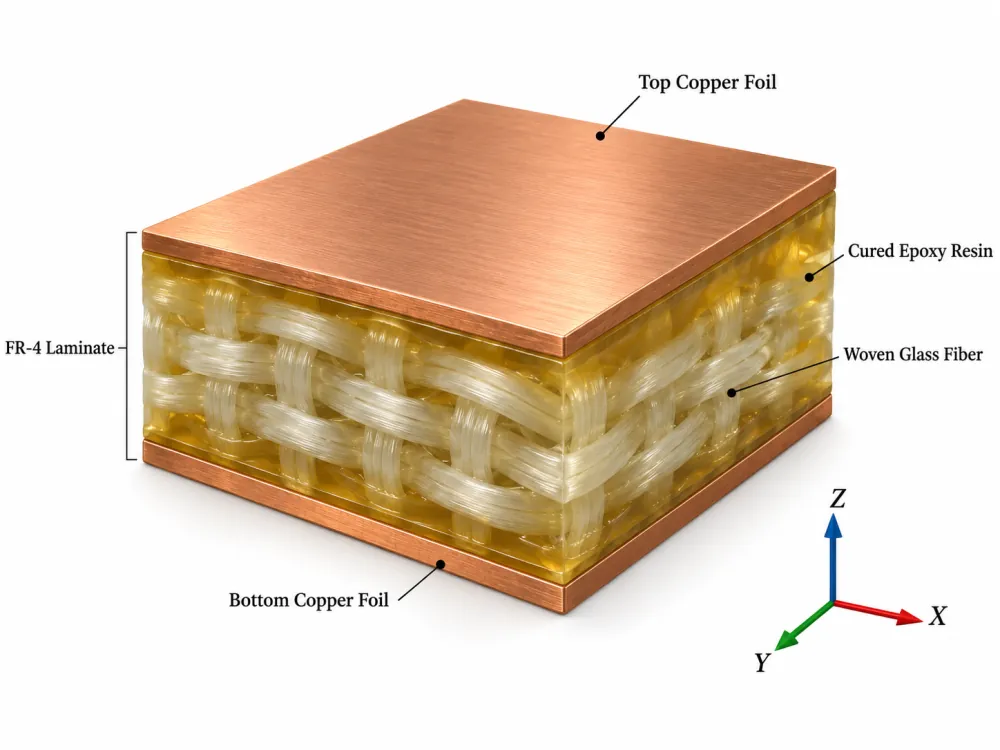
The FR-4 material properties that matter most depend on what your PCB must withstand: electrical signals, assembly heat, operating temperatures, voltage stress, moisture, and mechanical loading. Start with dielectric constant and loss, thermal expansion and stability, insulation performance, and mechanical requirements. FR-4 is a flame-retardant, glass-reinforced epoxy material class. It does not identify one fixed…
PCB 열 핫스팟 맵: 시뮬레이션 및 설계 수정
A PCB thermal hotspot map helps engineers find where heat concentrates before it becomes drift, derating, solder fatigue, or field failure. Instead of treating thermal review as a late-stage check, the map turns temperature into layout evidence: which packages, copper areas, vias, planes, and airflow routes carry the thermal load. For PCB engineers, the value…
PCB DFM Checklist
A PCB DFM checklist helps engineers and buyers catch manufacturability problems before a board is quoted, fabricated, assembled, or released to production. The goal is to confirm that the supplier can build the design with the required stackup, tolerances, finish, test plan, and documentation. DFM review reduces engineering holds and helps buyers compare suppliers. If…
PCB 비아 가이드: 유형, 설계 규칙 및 선택 팁
A PCB via is a plated interconnect that lets signals, power, ground, or heat move between copper layers in a printed circuit board. Via choice affects routing density, fabrication cost, assembly yield, signal integrity, and thermal performance, so it should be part of stackup and DFM planning, not a cleanup step at the end. For…

전력 PCB 및 전원 공급 장치 PCB 설계 가이드
A power PCB is the circuit board that receives, converts, regulates, distributes, or monitors electrical power. A power supply PCB is a more specific type of power PCB that converts an input source—such as AC mains, a battery, USB power, or a DC bus—into stable output voltage rails for an electronic product. The quality of…
FR4 PCB 가이드: FR4 소재 특성, 용도 및 설계 팁
FR-4 is the standard base material used for most printed circuit boards. It is a rigid composite made from woven glass cloth and epoxy resin, usually supplied as copper-clad laminate so copper circuits can be formed on one or both sides. An FR-4 PCB is therefore a circuit board built on an FR-4 substrate. It…