PCB設計
ここでは、PCB設計から組み立てまでの全工程に関する専門知識に加え、エレクトロニクス業界の最新動向を的確に分析する知識を身につけられます。
2026年版 AI PCB設計ソフトウェアおすすめ10選
最適なAI PCB設計ソフトウェアは、行いたい作業によって異なります。要件から回路図や部品表(BOM)を作成するのに役立つツールもあれば、既存の設計に対する部品配置、配線、検証を支援するツールもあります。生成されたレイアウトも、そのまま使えるわけではありません。回路を確認し、…に向けて仕上げるには、エンジニアによる確認が必要です。
アルミ基板:熱設計と材料
アルミ基板は、銅配線、電気絶縁性の熱伝導誘電体、アルミニウムベースを組み合わせたプリント基板です。誘電体は回路を電気的に絶縁しながら、熱を金属へ伝えます。この構造は、基板、取り付け部、冷却面が適切に熱を逃がせる構成の場合、LED照明やパワーエレクトロニクスに有効です。…
HDI PCB:積層構成、マイクロビア、設計
HDI PCB(高密度相互接続プリント基板)は、細い配線と小型の層間接続を使い、限られた面積により多くの配線を収めます。レーザーで開けたマイクロビアと薄いビルドアップ層により、接続ごとに基板を貫通する穴を使わずに、高密度部品パッドを接続できます。設計上の検討点は、こうした特徴が、対応する価値のある配線上の制約を解消するかどうかです。…

フレキシブルPCBの曲げ半径:計算方法と指定方法
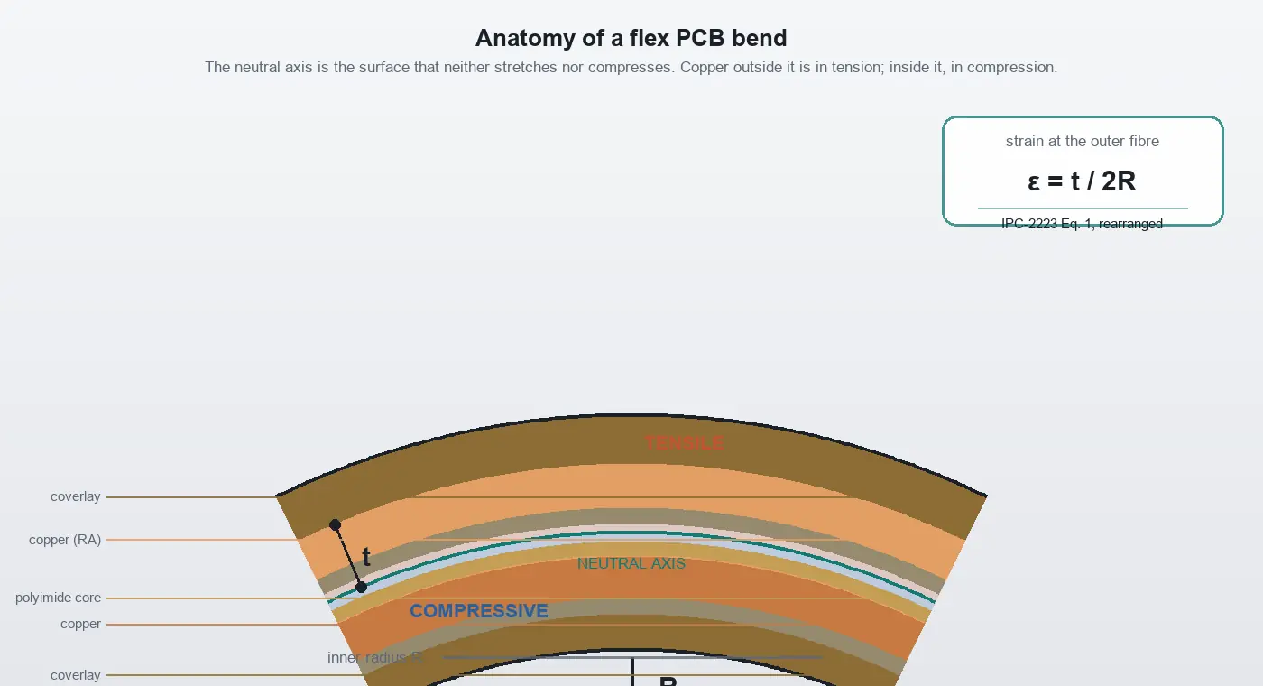
積層構成と筐体の寸法範囲が決まり、機械設計者からフレキシブルPCBの曲げ半径を求められたとします。その答えは一覧表を参照するだけでは得られません。必要なのはひずみ計算であり、表にある倍率は、積層構成を決めた後に計算から得られる値です。6×、10×、12×といった公表値はいずれも、…
2026年版 PCB設計ソフトウェアおすすめ10選
2026年にPCB設計ソフトウェアを選ぶエンジニアにとって、KiCadは無料で使えるデスクトップツールとして最も有力な出発点です。Altium Develop経由で利用するAltium Designerは、共有ライブラリ、ブラウザー上でのレビュー、電気・機械設計間の連携を1つの統合ワークフローで実現したい小規模チームに適した有料製品です。どちらも本格的な基板設計に対応しています。購入を決める際のポイントは、それぞれの周辺ワークフローが…かどうかです。
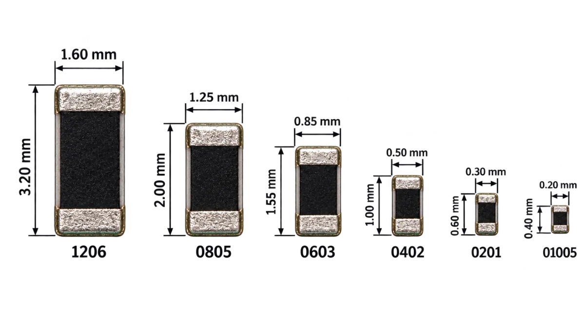
SMD抵抗器ガイド:コード、サイズ、フットプリント、定格
SMD抵抗器は、リードのない長方形のパッケージに収められた固定抵抗器で、プリント基板の穴に通すのではなく、基板表面のランドにはんだ付けします。一般に、基板上で最も数が多く、データシートではなく慣例に基づいて指定されることが最も多い部品です。多くのガイドでは…
QFNパッケージとは?PCB設計・実装の実践ガイド
QFN packages appear in everything from power supplies and wireless modules to sensors, microcontrollers, and automotive electronics. Their small footprint, short electrical paths, and efficient heat transfer make them an attractive alternative to larger leaded packages. However, the same underside connections that save space also make QFN footprint design, soldering, and inspection less forgiving. So,…

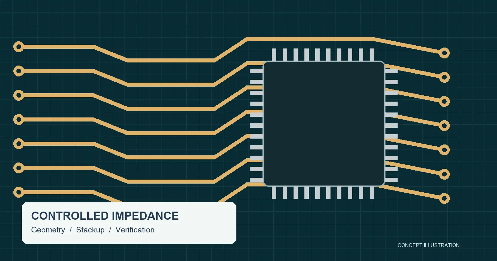
インピーダンス制御PCB設計:スタックアップ、仕様、試験
Controlled impedance is the practice of designing and manufacturing PCB traces so their characteristic impedance meets a specified target and tolerance. The result depends on the conductor geometry, dielectric construction, and reference planes. A complete requirement also states how the manufacturer will verify the finished structure. A note that says only “50 ohms” leaves important…
10kΩ抵抗器:カラーコード、用途、適切な選び方
A 10k resistor is a passive electrical component with a nominal resistance of 10,000 ohms (10kΩ). In modern circuit design, it is one of the most ubiquitous values found on breadboards and production PCBs alike. Engineers and hobbyists turn to 10k resistors because they hit an ideal electrical middle ground: they limit current to safe,…

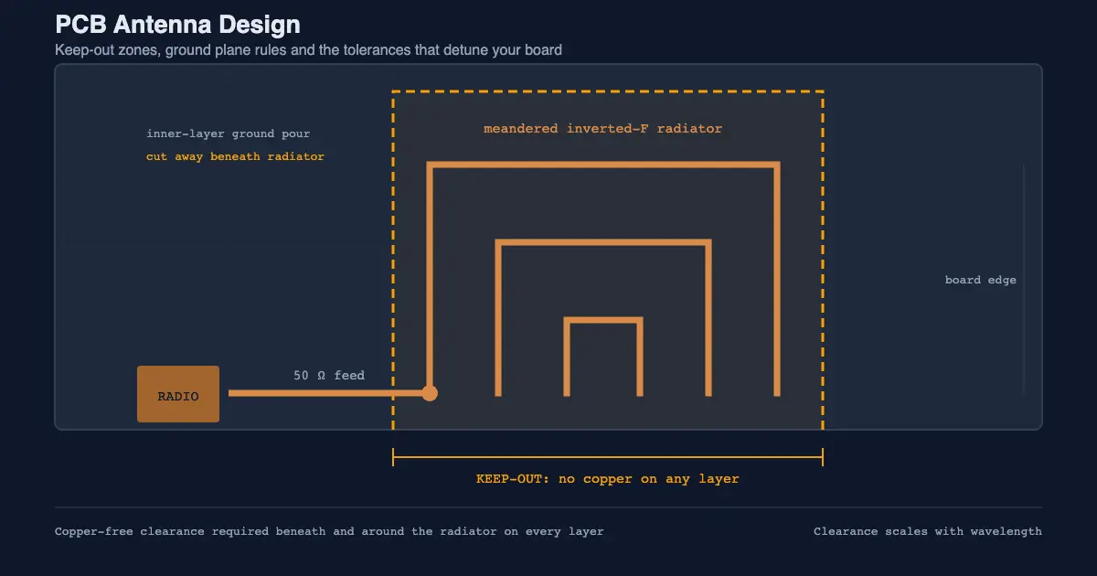
PCBアンテナ設計:レイアウト、材料、製造
A PCB antenna is a copper trace or pattern etched directly onto a printed circuit board that transmits and receives radio frequency electromagnetic waves. It is the cheapest way to give a product wireless connectivity, because it adds no connector, no cable and no bill-of-materials line. It is also the part of a design most…
PCBラミネート選定のためのFR-4材料特性
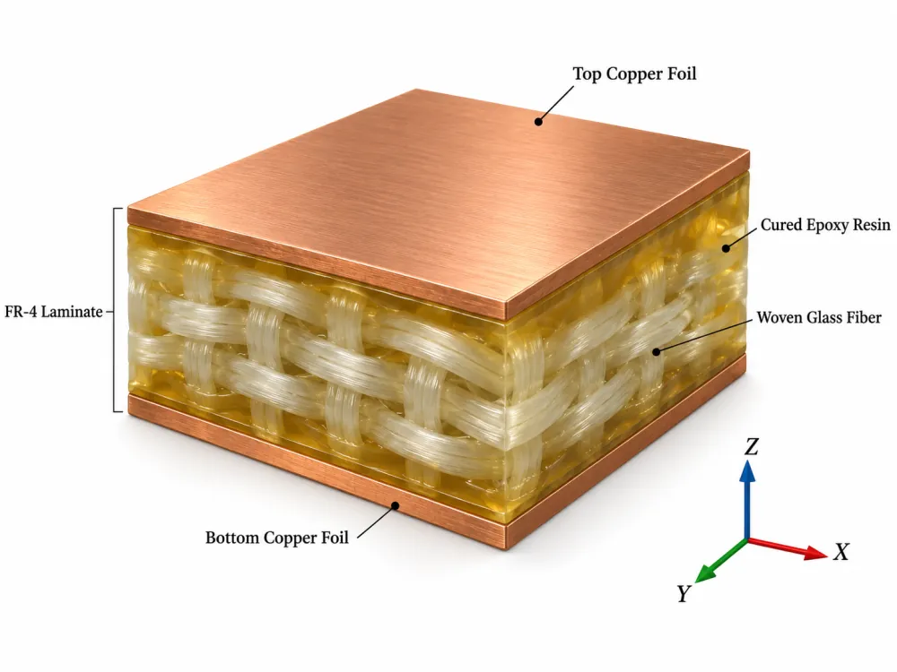
The FR-4 material properties that matter most depend on what your PCB must withstand: electrical signals, assembly heat, operating temperatures, voltage stress, moisture, and mechanical loading. Start with dielectric constant and loss, thermal expansion and stability, insulation performance, and mechanical requirements. FR-4 is a flame-retardant, glass-reinforced epoxy material class. It does not identify one fixed…
PCB熱ホットスポットマップ:シミュレーションと設計改善
A PCB thermal hotspot map helps engineers find where heat concentrates before it becomes drift, derating, solder fatigue, or field failure. Instead of treating thermal review as a late-stage check, the map turns temperature into layout evidence: which packages, copper areas, vias, planes, and airflow routes carry the thermal load. For PCB engineers, the value…
PCB DFM Checklist
A PCB DFM checklist helps engineers and buyers catch manufacturability problems before a board is quoted, fabricated, assembled, or released to production. The goal is to confirm that the supplier can build the design with the required stackup, tolerances, finish, test plan, and documentation. DFM review reduces engineering holds and helps buyers compare suppliers. If…
PCBビアガイド:種類、設計ルール、選び方のヒント
A PCB via is a plated interconnect that lets signals, power, ground, or heat move between copper layers in a printed circuit board. Via choice affects routing density, fabrication cost, assembly yield, signal integrity, and thermal performance, so it should be part of stackup and DFM planning, not a cleanup step at the end. For…

パワーPCBと電源PCBの設計ガイド
A power PCB is the circuit board that receives, converts, regulates, distributes, or monitors electrical power. A power supply PCB is a more specific type of power PCB that converts an input source—such as AC mains, a battery, USB power, or a DC bus—into stable output voltage rails for an electronic product. The quality of…
FR4基板ガイド:FR4の材料特性、用途、設計のヒント
FR-4 is the standard base material used for most printed circuit boards. It is a rigid composite made from woven glass cloth and epoxy resin, usually supplied as copper-clad laminate so copper circuits can be formed on one or both sides. An FR-4 PCB is therefore a circuit board built on an FR-4 substrate. It…