PCB 제작
여기에서 PCB 설계부터 조립까지 전 과정을 아우르는 전문 지식과 전자 산업의 최신 동향에 대한 정확한 분석을 얻을 수 있습니다.
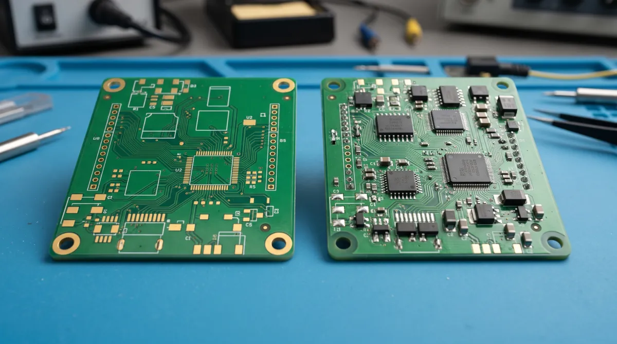
PCB와 PCBA의 차이점은 무엇인가요?
PCB vs PCBA comes down to the deliverable: in a manufacturing order, a PCB commonly means a bare printed circuit board, while PCBA can mean the assembly process or the board after components have been mounted. A populated board is not automatically programmed, functionally tested, or ready to install in a finished product. The terms…
드론에 사용되는 회로 기판의 종류와 각 기판의 역할
드론에 사용되는 회로 기판에는 비행 제어기, 전자식 속도 제어기, 전력 분배 기판, 센서 및 항법 기판, 통신 기판, 카메라 또는 기타 탑재체용 기판이 있습니다. 일부 드론은 이러한 기능 여러 가지를 하나의 어셈블리에 통합하고, 다른 드론은 별도의 모듈을 연결합니다. 각 기능은 인쇄회로기판(PCB)에 서로 다른 요구 사항을 부과합니다.…

유럽 PCB 제조업체 상위 10곳 (2026)
유럽의 PCB 제조업체를 선정할 때는 실제로 베어 보드가 어디에서 제작되는지부터 확인해야 합니다. 유럽에 있는 사무실, 조립 라인, 기판 제조 공장은 서로 다른 시설입니다. 이 목록에서는 유럽 내 지정된 사업장에서 PCB를 생산한다는 근거가 있는 10개 업체를 소개하고, 견적을 요청하기 전에 확인해야 할 사항을 설명합니다.…

리지드 플렉스 PCB 설계: 적층 구조, 전환부 및 비용
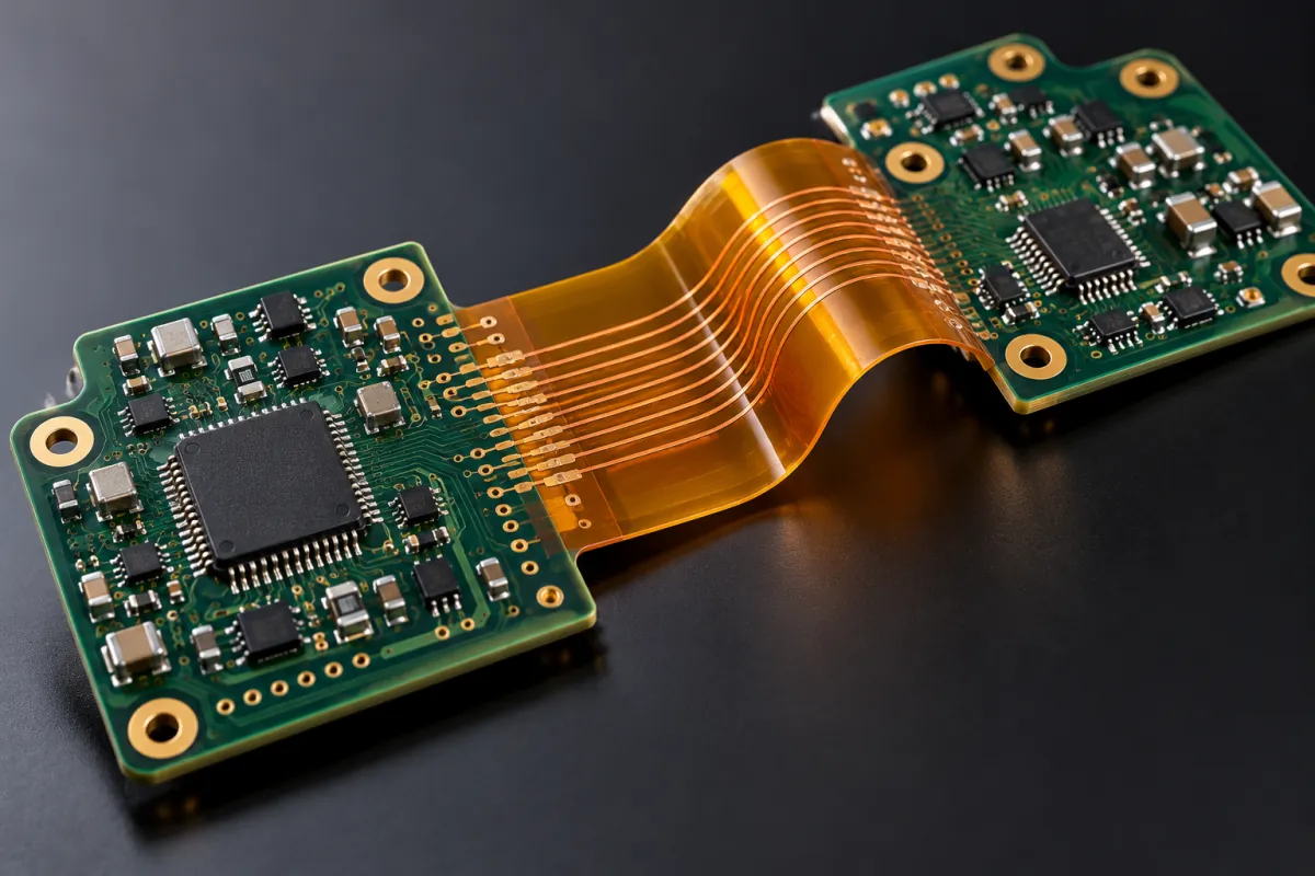
리지드 플렉스 PCB는 하나의 구조에 경성 회로 영역과 연성 회로층을 결합한 기판입니다. 경성 영역은 부품을 지지하고 추가 전도층을 포함할 수 있으며, 연성 영역은 외함 안에서 이 영역들을 연결합니다. 도체는 리지드-플렉스 전환부를 가로질러 신호와 전력을 영역 간에 전달합니다. 부품이 실장된 소형 제어 장치의 가상 사례를 생각해 보겠습니다.…
표준 PCB 두께: 치수, 공차 및 커넥터 결합
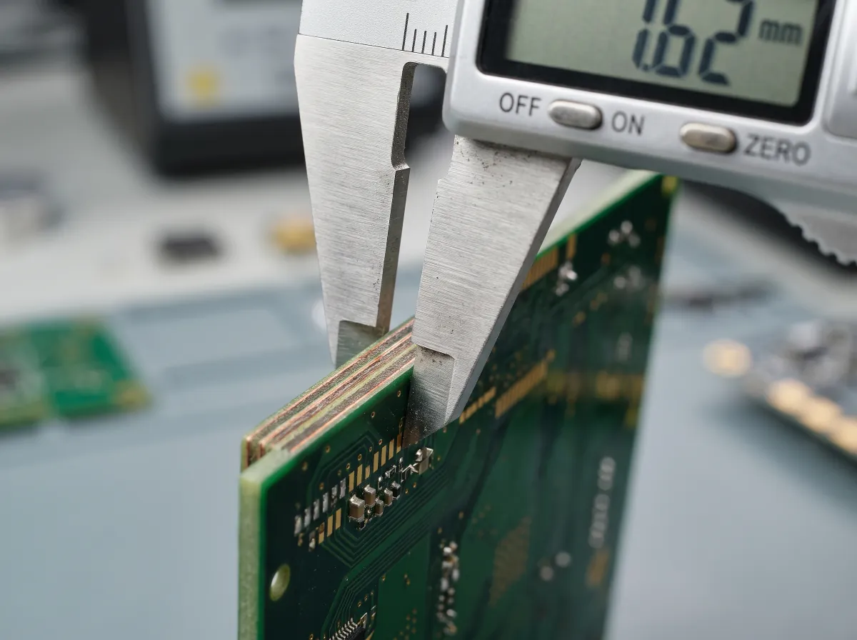
범용 경성 기판 다수에 적용되는 표준 PCB 두께는 완성 두께 기준 공칭 1.6 mm이며, 약 0.063인치 또는 63밀입니다. 2026년 9월 9일에 업데이트된 JLCPCB의 표준 PCB 두께 안내에서는 1.6 mm를 일반적인 표준 두께로 소개합니다. Altium의 기판 두께 및 적층 구조 안내에도 설명되어 있듯이 다른 두께도 사용됩니다. 공칭값은…
다층 PCB: 적층 구조, 비용 및 설계
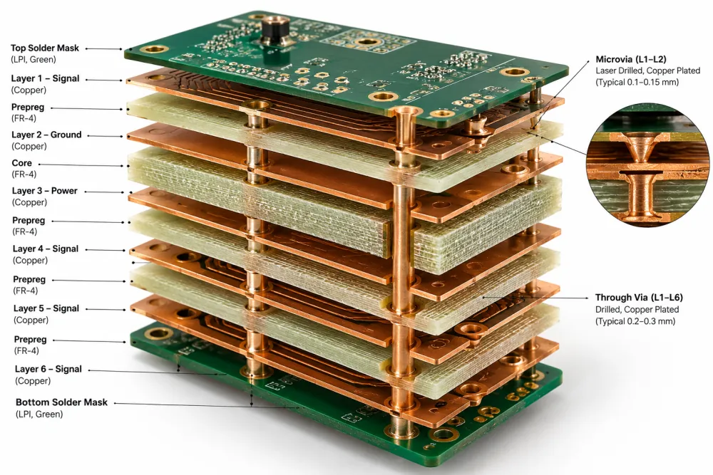
다층 PCB는 절연 유전체로 분리된 구리 도전층이 세 개 이상 포함되며, 이 층들을 접합해 하나의 기판으로 만든 것입니다. 층수는 구리층을 기준으로 하며, 프리프레그, 코어 시트 또는 솔더 마스크는 포함하지 않습니다. 층수만으로는 기판이 경성인지 연성인지, 두께가 얼마인지, 또는 얼마나 잘 작동할지 알 수 없습니다.…
산업용 PCB 생산: 공정 및 품질 보증
산업용 PCB 생산은 승인된 회로 기판 설계를 베어 보드로 제작하고, 주문에 따라 산업 장비용 부품 실장 어셈블리까지 만드는 과정입니다. 제작 공정에는 기판 제조, 부품 조립, 검사 및 합의된 시험이 포함됩니다. 승인 여부는 지정된 제작 사양, 작동 조건 및 합격 기준에 따라 결정됩니다. 모터 컨트롤러, 센서 인터페이스, 제어반 장착 기판에는 서로 다른 재료와 기계적 지지 방식이 필요할 수 있습니다.…
HDI PCB: 적층 구조, 마이크로비아 및 설계
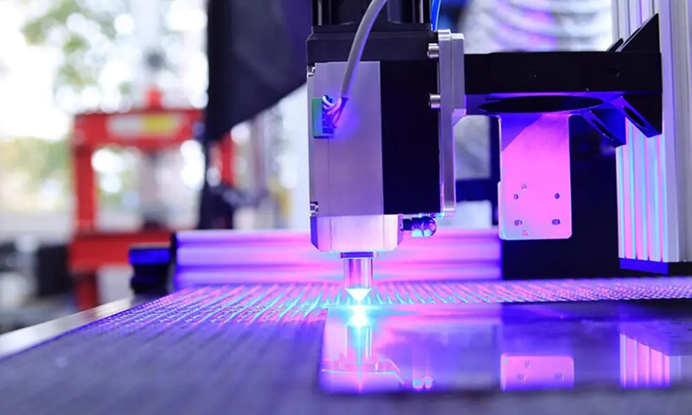
HDI PCB(고밀도 상호 연결 인쇄회로기판)는 가는 도체와 소형 층간 연결부를 사용해 주어진 면적에 더 많은 배선을 배치합니다. 레이저로 가공한 마이크로비아와 얇은 빌드업층은 모든 연결부에 관통 구멍을 사용하지 않고도 조밀한 부품 패드를 서로 연결할 수 있게 합니다. 설계에서 고려할 점은 이러한 특징이 배선 제약을 해결할 만큼의 가치가 있는지입니다.…

리지드 PCB: 재료, 구조 및 설계 선택
리지드 PCB, 즉 경성 인쇄회로기판은 사용 중 형태를 유지하도록 설계된 기판 위의 구리 도체를 통해 부품을 지지하고 연결합니다. 사용 중 휘어지는 것이 아니라 외함 안에 회로가 고정되는 전자 제품에 적합합니다. 기판을 선택할 때는 구조를 회로, 장착 방식, 커넥터 및 사용 환경에 맞춰야 합니다. 층…

플렉스 PCB: 유형, 재료, 적층 구조 및 설계 규칙
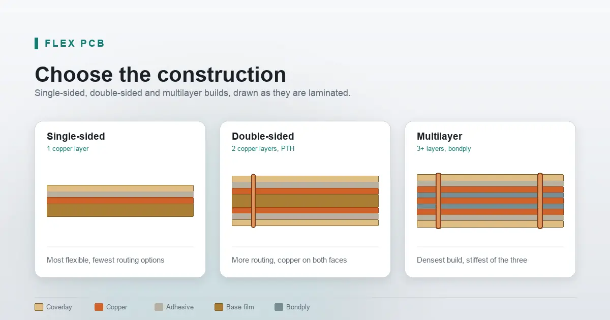
플렉스 PCB는 일반적으로 폴리이미드와 같은 유연한 폴리머 필름 위에 구리 도체를 접합하고, 커버레이로 보호한 회로입니다. 이것이 정의이며, 검색 결과 상단에서 이미 답을 얻을 수 있는 부분입니다. 하지만 실제 제작물이 제대로 작동할지를 결정하는 것은 이 정의가 아닙니다. 다음 네 가지 질문이 그 답을 좌우합니다.…
플렉스 PCB 굽힘 반경: 계산 및 지정 방법
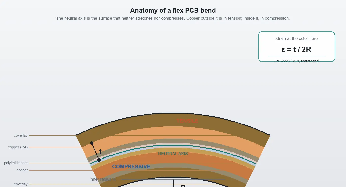
적층 구조와 하우징 공간이 정해졌고, 기구 설계 엔지니어가 플렉스 PCB의 굽힘 반경을 묻고 있습니다. 답은 단순한 표에서 찾을 수 있는 값이 아닙니다. 이는 변형률 계산의 결과이며, 표에 나온 배수는 적층 구조를 정한 뒤 계산으로 얻는 값입니다. 6×, 10×, 12× 등으로 표시되는 모든 공개 배수는…
리플로우 납땜 안내: 공정, 프로파일 및 결함
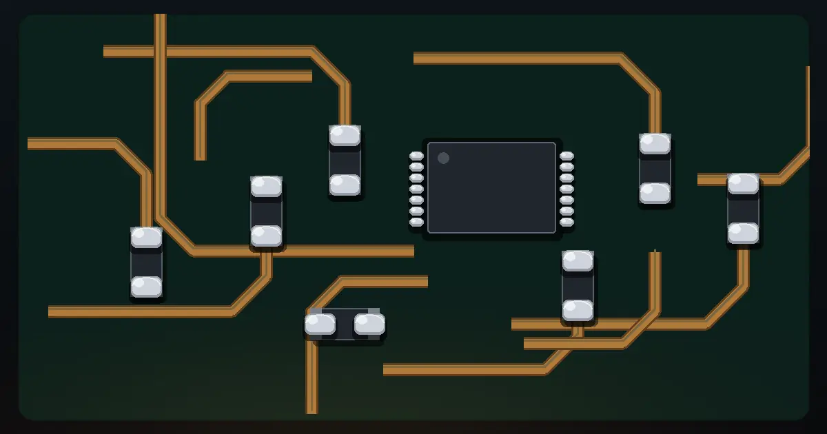
리플로우 납땜은 스텐실로 인쇄한 솔더 페이스트를 가열해 녹이고, 부품 단자에 젖어 들게 한 뒤 냉각하면서 접합부를 형성해 표면 실장 부품을 인쇄회로기판에 부착하는 공정입니다. 거의 모든 현대 전자 제품에서 주요 조립 방식으로 사용되며, 가장 큰 비용 손실을 초래하는 실수가 발생하기 쉬운 단계이기도 합니다.…
동박 적층판(CCL): 유형, 제조, 성능 및 표준
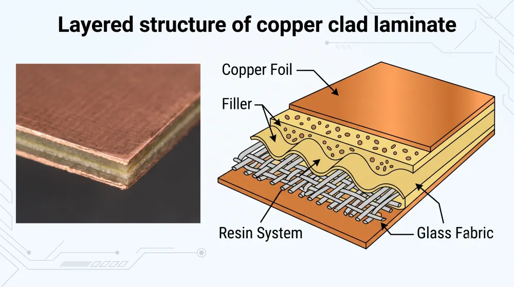
동박적층판(CCL)은 PCB의 도체를 형성하는 기본 소재입니다. 구리박을 경화된 유리섬유 강화 에폭시, 유연한 고분자 필름 또는 금속 베이스의 열전도성 유전체와 같은 절연 소재에 접합해 만듭니다. 일반적인 다층 경성 PCB에서는 패턴이 형성된 CCL이 코어가 되는 경우가 많습니다.…
JLCPCB vs PCBWay: 프로젝트에 적합한 PCB 제조업체는? (2026)
For a straightforward PCB prototype or a small assembly order that fits JLCPCB’s Economic PCBA rules, start with JLCPCB, especially when the components are already in its inventory. For rigid-flex or extensive custom fabrication requirements, shortlist PCBWay early. These recommendations follow from JLCPCB’s economical assembly tier and PCBWay’s documented advanced manufacturing options. The JLCPCB vs…

관통 구멍이란? PCB 유형, 용도 및 설계 가이드
A through hole is an opening that passes completely from one side of a printed circuit board (PCB) to the other. It may be plated with conductive copper to create an electrical connection, or left unplated for mechanical use. Through holes are commonly used for component leads, connectors, vias, mounting hardware, alignment pins, and slots.…

PCB 소재 가이드: 종류, 특성 및 선택
PCB material affects far more than the physical strength of a circuit board. It influences impedance, signal loss, heat dissipation, dimensional stability, assembly reliability, manufacturability, lead time, and cost. A material that works well for a basic controller may fail in a 77 GHz radar module, a high-current LED board, or a rigid-flex medical device.…

PCB 공급업체 자격 심사 체크리스트 [2026 Guide]
A PCB supplier qualification checklist helps engineers and buyers verify whether a PCB fabricator, PCBA supplier, or EMS partner can meet the product's technical, quality, delivery, and documentation requirements before production starts. ISO describes ISO 9001:2015 as a globally recognized quality management standard for improving performance and maintaining a quality management system (ISO, 2026). In…
PCB DFM Checklist
A PCB DFM checklist helps engineers and buyers catch manufacturability problems before a board is quoted, fabricated, assembled, or released to production. The goal is to confirm that the supplier can build the design with the required stackup, tolerances, finish, test plan, and documentation. DFM review reduces engineering holds and helps buyers compare suppliers. If…