전자 회로
여기에서 PCB 설계부터 조립까지 전 과정을 아우르는 전문 지식과 전자 산업의 최신 동향에 대한 정확한 분석을 얻을 수 있습니다.
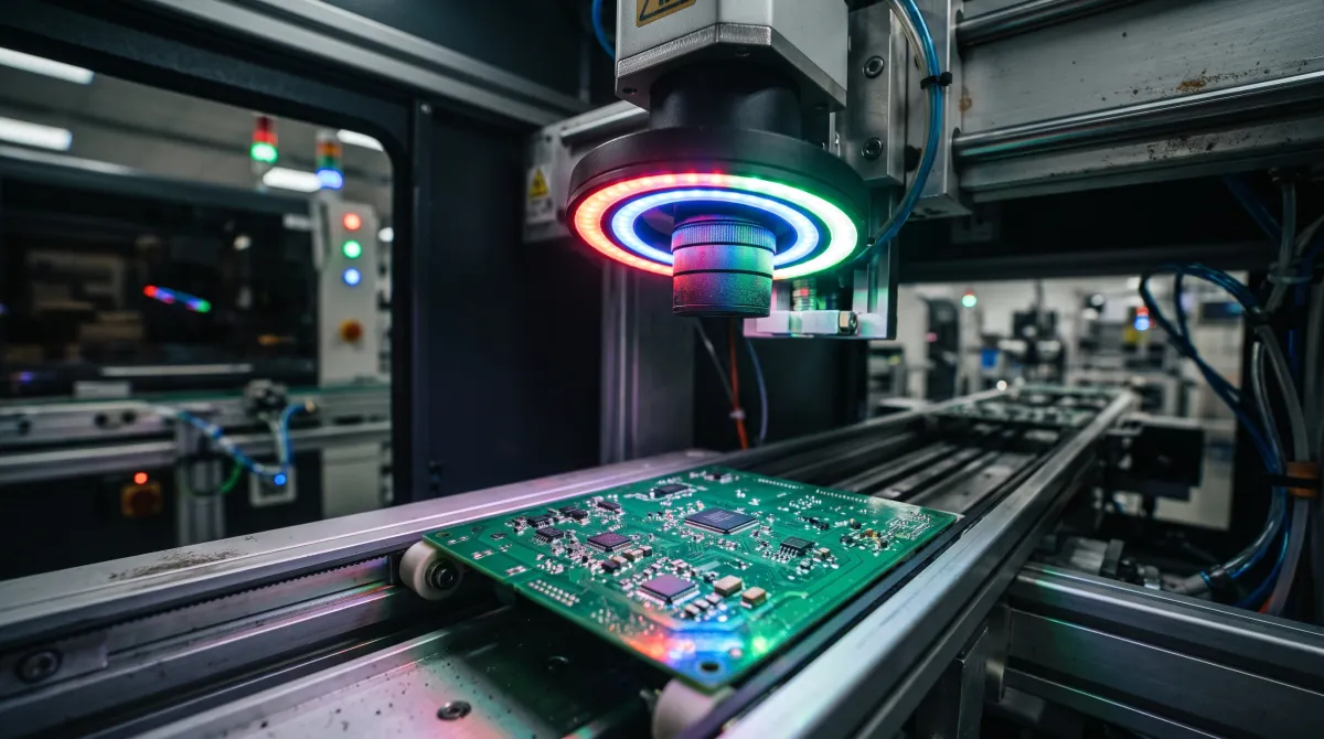
AOI란 무엇인가요? PCB 자동 광학 검사
AOI란 무엇인가요? 자동 광학 검사(AOI)는 카메라, 조명, 소프트웨어를 사용해 회로 기판에 지정된 외관상 특징이나 잠재적 결함이 있는지 확인합니다. PCB 조립 과정에서는 부품 누락이나 납땜 브리지 노출을 감지할 수 있습니다. AOI는 베어 보드의 구리 패턴도 검사할 수 있지만, 숨겨진 접합부를 모두 확인하거나 기판이 정상 작동하는지 판별할 수는 없습니다.…
드론에 사용되는 회로 기판의 종류와 각 기판의 역할
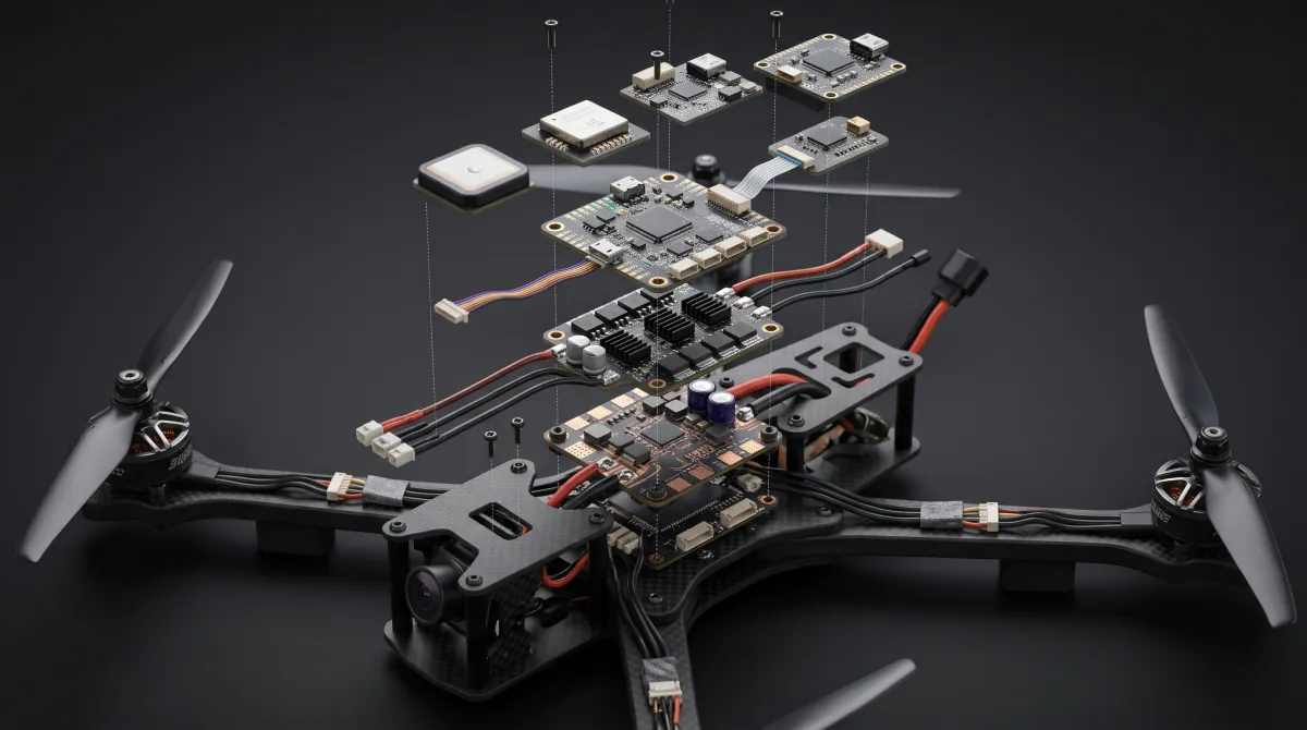
드론에 사용되는 회로 기판에는 비행 제어기, 전자식 속도 제어기, 전력 분배 기판, 센서 및 항법 기판, 통신 기판, 카메라 또는 기타 탑재체용 기판이 있습니다. 일부 드론은 이러한 기능 여러 가지를 하나의 어셈블리에 통합하고, 다른 드론은 별도의 모듈을 연결합니다. 각 기능은 인쇄회로기판(PCB)에 서로 다른 요구 사항을 부과합니다.…
IPC J-STD-001: 납땜 요구사항 안내
IPC J-STD-001, 「납땜된 전기 및 전자 어셈블리 요구사항」은 납땜 어셈블리의 재료, 공정 및 합격 기준에 관한 요구사항을 규정합니다. 어셈블리 제작 방법뿐 아니라 완성된 접합부에 대한 요구사항도 다룹니다. 구매 주문서에 이 표준을 명시할 때는 적용할 개정판, 제품 등급 및 프로젝트별 요구사항을 지정해야 합니다. 어셈블리 구매 담당자에게는…
산업용 PCB 생산: 공정 및 품질 보증
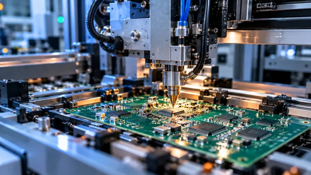
산업용 PCB 생산은 승인된 회로 기판 설계를 베어 보드로 제작하고, 주문에 따라 산업 장비용 부품 실장 어셈블리까지 만드는 과정입니다. 제작 공정에는 기판 제조, 부품 조립, 검사 및 합의된 시험이 포함됩니다. 승인 여부는 지정된 제작 사양, 작동 조건 및 합격 기준에 따라 결정됩니다. 모터 컨트롤러, 센서 인터페이스, 제어반 장착 기판에는 서로 다른 재료와 기계적 지지 방식이 필요할 수 있습니다.…
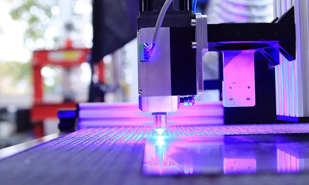
리플로우 납땜 안내: 공정, 프로파일 및 결함
리플로우 납땜은 스텐실로 인쇄한 솔더 페이스트를 가열해 녹이고, 부품 단자에 젖어 들게 한 뒤 냉각하면서 접합부를 형성해 표면 실장 부품을 인쇄회로기판에 부착하는 공정입니다. 거의 모든 현대 전자 제품에서 주요 조립 방식으로 사용되며, 가장 큰 비용 손실을 초래하는 실수가 발생하기 쉬운 단계이기도 합니다.…
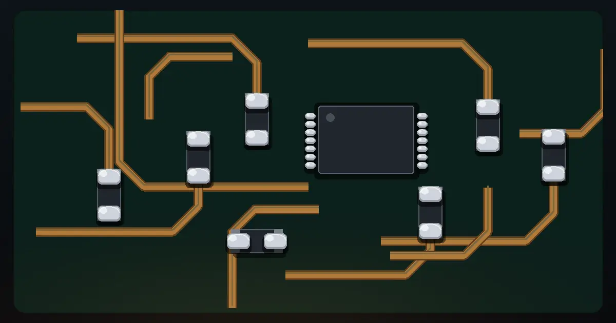
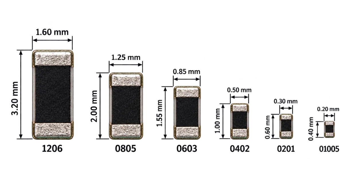
SMD 저항기 안내: 코드, 크기, 풋프린트 및 한계
SMD 저항기는 리드가 없는 직사각형 패키지의 고정값 저항기로, 구멍에 삽입하는 대신 인쇄회로기판 표면의 패드에 납땜됩니다. 일반적으로 기판에서 가장 수가 많은 부품이면서 데이터시트보다 관행에 따라 사양이 정해지는 경우가 가장 많은 부품이기도 합니다. 대부분의 안내 자료는…
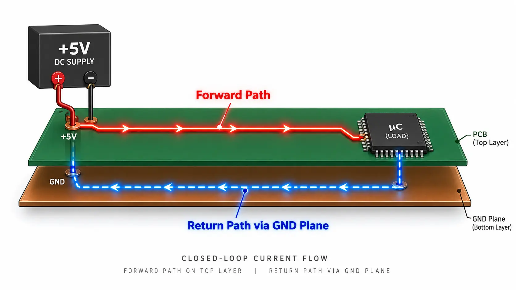
GND란 무엇인가요? 의미, 종류 및 PCB 접지 설명
GND appears on almost every circuit diagram, PCB, power supply, and electronic module. It is often described as “zero volts” or “the negative terminal,” but neither description is universally correct. In electronics, GND stands for ground. It is the reference node against which other voltages are measured and, in many circuits, part of the path…
관통 구멍이란? PCB 유형, 용도 및 설계 가이드
A through hole is an opening that passes completely from one side of a printed circuit board (PCB) to the other. It may be plated with conductive copper to create an electrical connection, or left unplated for mechanical use. Through holes are commonly used for component leads, connectors, vias, mounting hardware, alignment pins, and slots.…

LED 애노드와 캐소드: 양극 및 음극 단자를 식별하는 방법
An LED (Light Emitting Diode) is a polarized semiconductor device that allows current to flow in only one direction. To illuminate an LED, you must connect its positive and negative terminals correctly within your circuit. On standard through-hole LEDs, the longer leg and the rounded side represent the anode, while the shorter leg and the…

0402 Resistors Guide: Size, Specs, and Selection
Hardware design always comes down to a battle for board space. As consumer wearables, IoT devices, and high-performance computing modules pack more features into smaller enclosures, printed circuit board (PCB) real estate has become an incredibly valuable commodity. Moving away from legacy through-hole parts and bulkier surface-mount devices (SMDs) is no longer optional—it is a…
IPC-TM-650 설명: PCB 시험 방법, 주요 절차 및 품질 활용
“Test to IPC” is not a complete PCB requirement. A supplier still needs the method, revision, samples, conditions, and acceptance criteria before it can quote or run the work. IPC-TM-650 is the procedure side of PCB testing. It helps engineers choose a way to measure a board characteristic. The governing specification, drawing, or contract still…

PCB 라미네이트 선택을 위한 FR-4 재료 특성
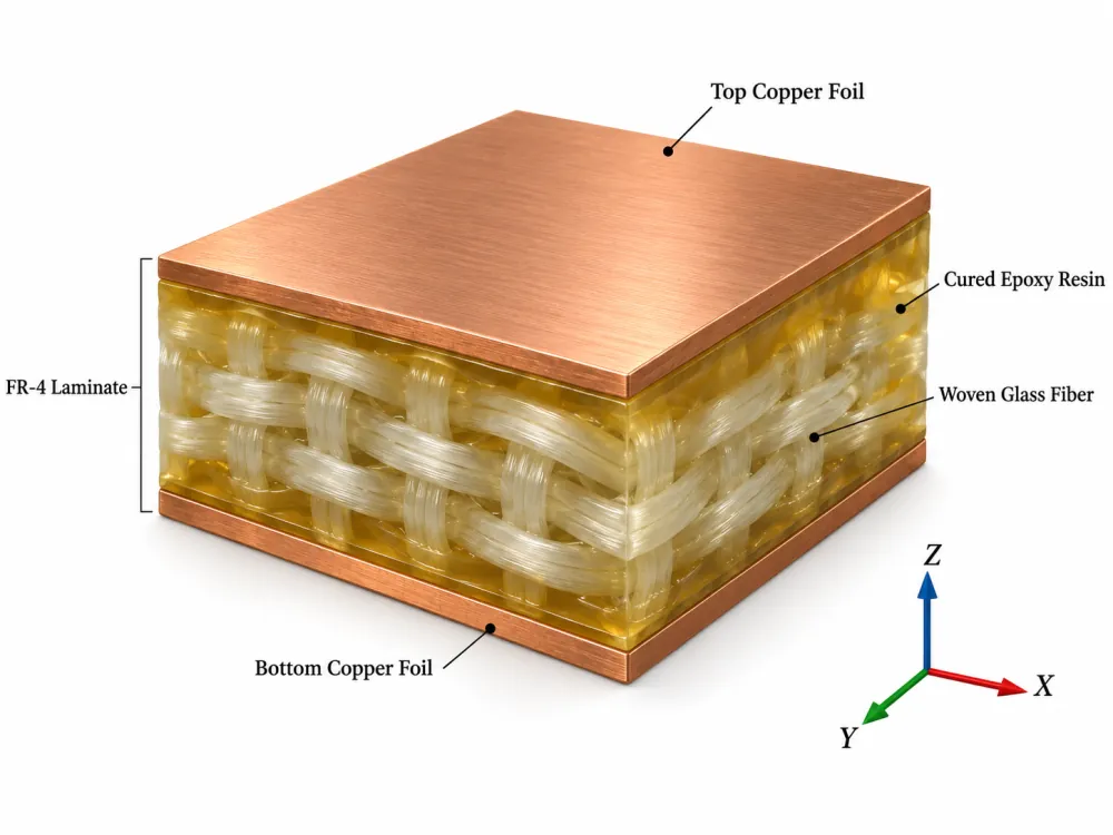
The FR-4 material properties that matter most depend on what your PCB must withstand: electrical signals, assembly heat, operating temperatures, voltage stress, moisture, and mechanical loading. Start with dielectric constant and loss, thermal expansion and stability, insulation performance, and mechanical requirements. FR-4 is a flame-retardant, glass-reinforced epoxy material class. It does not identify one fixed…
PCB 비아 가이드: 유형, 설계 규칙 및 선택 팁
A PCB via is a plated interconnect that lets signals, power, ground, or heat move between copper layers in a printed circuit board. Via choice affects routing density, fabrication cost, assembly yield, signal integrity, and thermal performance, so it should be part of stackup and DFM planning, not a cleanup step at the end. For…

전력 PCB 및 전원 공급 장치 PCB 설계 가이드
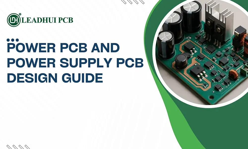
A power PCB is the circuit board that receives, converts, regulates, distributes, or monitors electrical power. A power supply PCB is a more specific type of power PCB that converts an input source—such as AC mains, a battery, USB power, or a DC bus—into stable output voltage rails for an electronic product. The quality of…
SMT의 의미: 표면 실장 기술 알아보기
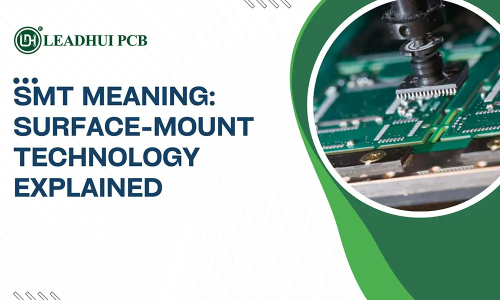
SMT means Surface-Mount Technology: a method of attaching electronic components directly onto the surface of a printed circuit board (PCB). Rather than inserting long component leads through drilled holes, SMT uses small surface-mount components that are placed on solder-coated pads and permanently connected through controlled heating. In practical terms, SMT is what makes modern electronics…
듀얼 인라인 패키지의 의미: 핀 배열, 치수 및 조립 가이드
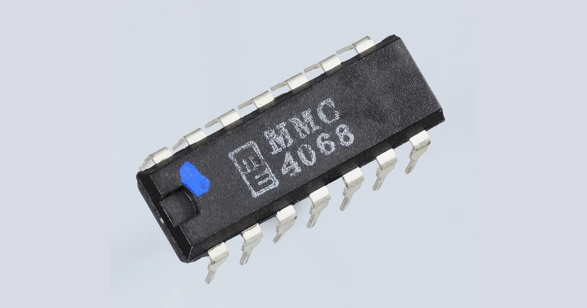
A dual inline package (DIP) is a component package with two parallel rows of leads. Many DIPs are inserted into holes in a circuit board or a socket. The package describes the part's physical form; it does not tell you what the circuit inside does. For a board designer, identifying a DIP is only the…