PCB 조립
여기에서 PCB 설계부터 조립까지 전 과정을 아우르는 전문 지식과 전자 산업의 최신 동향에 대한 정확한 분석을 얻을 수 있습니다.
표면 실장과 스루홀: 주요 차이점, 비용 및 선택 방법
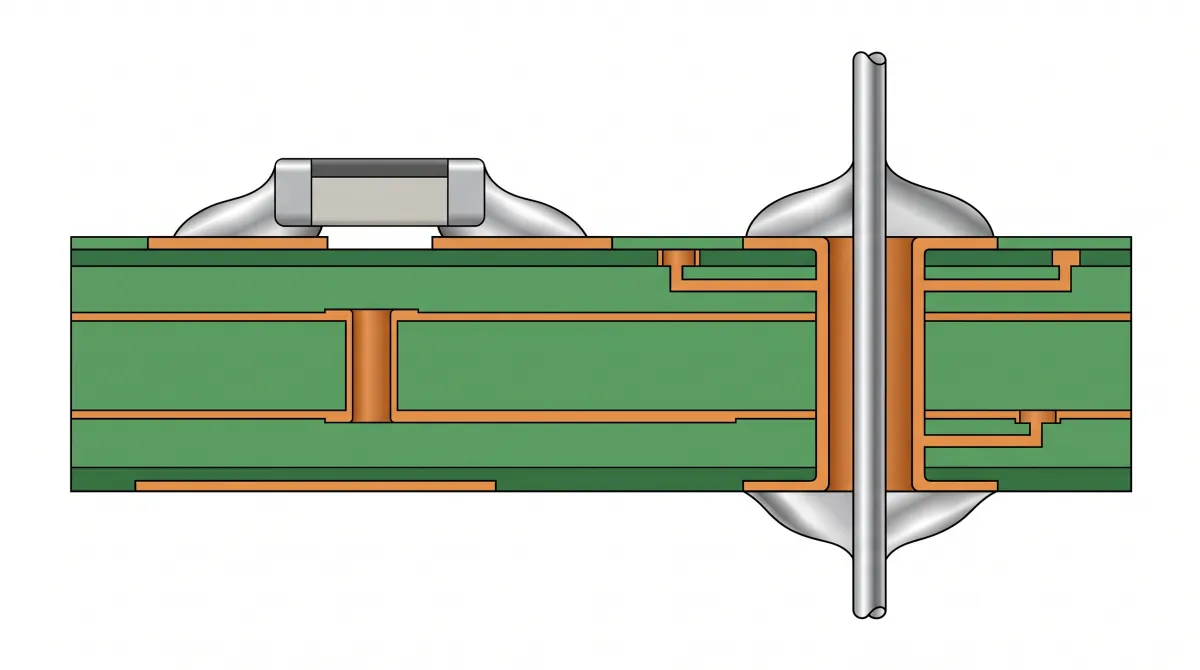
Surface-mount components attach to pads on a circuit board's surface. Through-hole components have leads that pass into holes in the board for soldering. Surface-mount technology (SMT) often suits compact layouts and automated assembly; through-hole technology (THT) can be useful when a selected component or its mechanical load calls for it. Many boards use both. The…
PCB와 PCBA의 차이점은 무엇인가요?
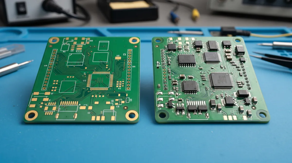
PCB vs PCBA comes down to the deliverable: in a manufacturing order, a PCB commonly means a bare printed circuit board, while PCBA can mean the assembly process or the board after components have been mounted. A populated board is not automatically programmed, functionally tested, or ready to install in a finished product. The terms…
PCB용 솔더 플럭스: 종류, 용도 및 세척 방법
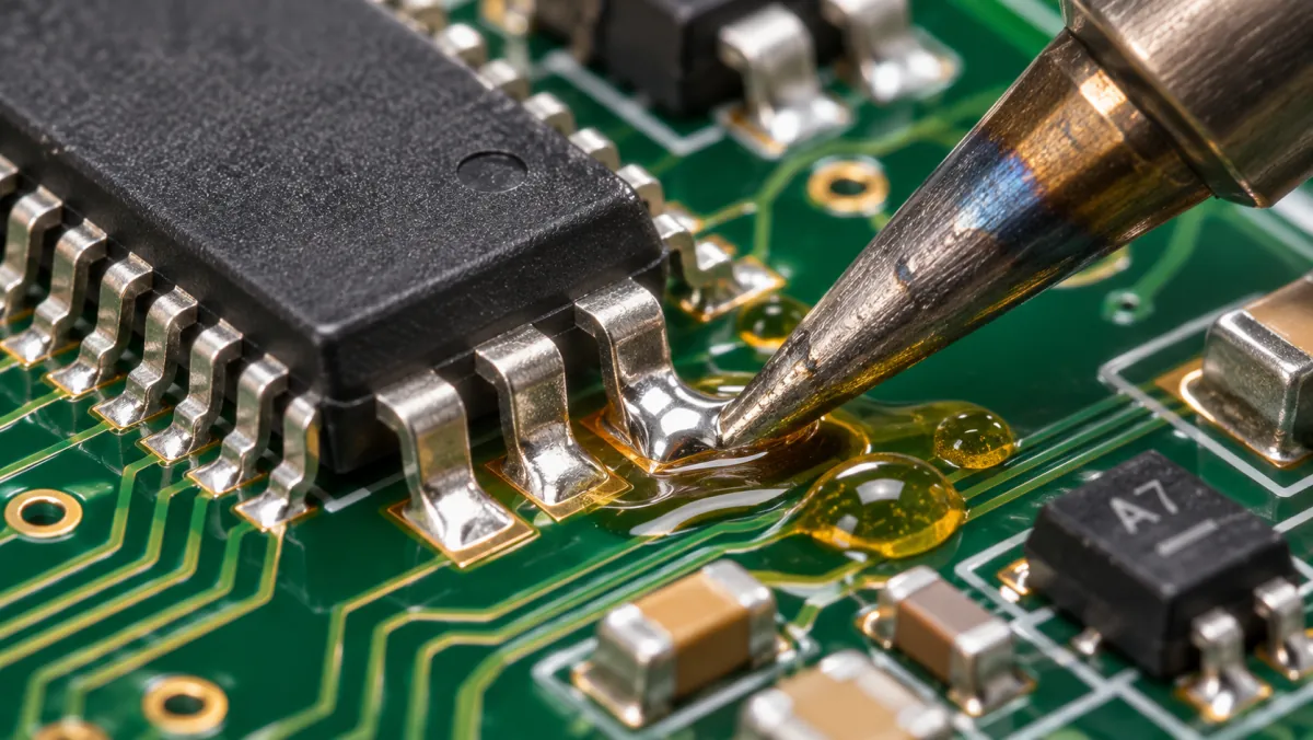
솔더 플럭스는 금속 표면의 산화물을 제거하고 가열 중 산화가 다시 진행되는 것을 억제해 납땜이 금속 표면에 잘 젖어 들도록 돕는 화학 조성물입니다. 인쇄회로기판 조립에서는 별도로 도포하거나 솔더 와이어 또는 솔더 페이스트에 포함된 형태로 사용할 수 있습니다. 플럭스의 선택은 접합부 형성 방식뿐 아니라 남는 잔류물에도 영향을 줍니다.…
IPC J-STD-001: 납땜 요구사항 안내
IPC J-STD-001, 「납땜된 전기 및 전자 어셈블리 요구사항」은 납땜 어셈블리의 재료, 공정 및 합격 기준에 관한 요구사항을 규정합니다. 어셈블리 제작 방법뿐 아니라 완성된 접합부에 대한 요구사항도 다룹니다. 구매 주문서에 이 표준을 명시할 때는 적용할 개정판, 제품 등급 및 프로젝트별 요구사항을 지정해야 합니다. 어셈블리 구매 담당자에게는…
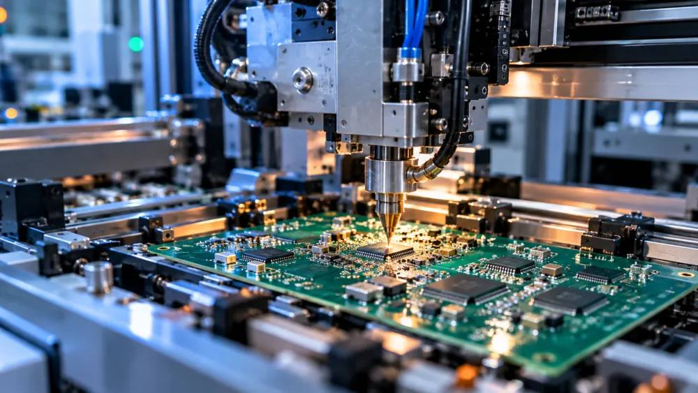
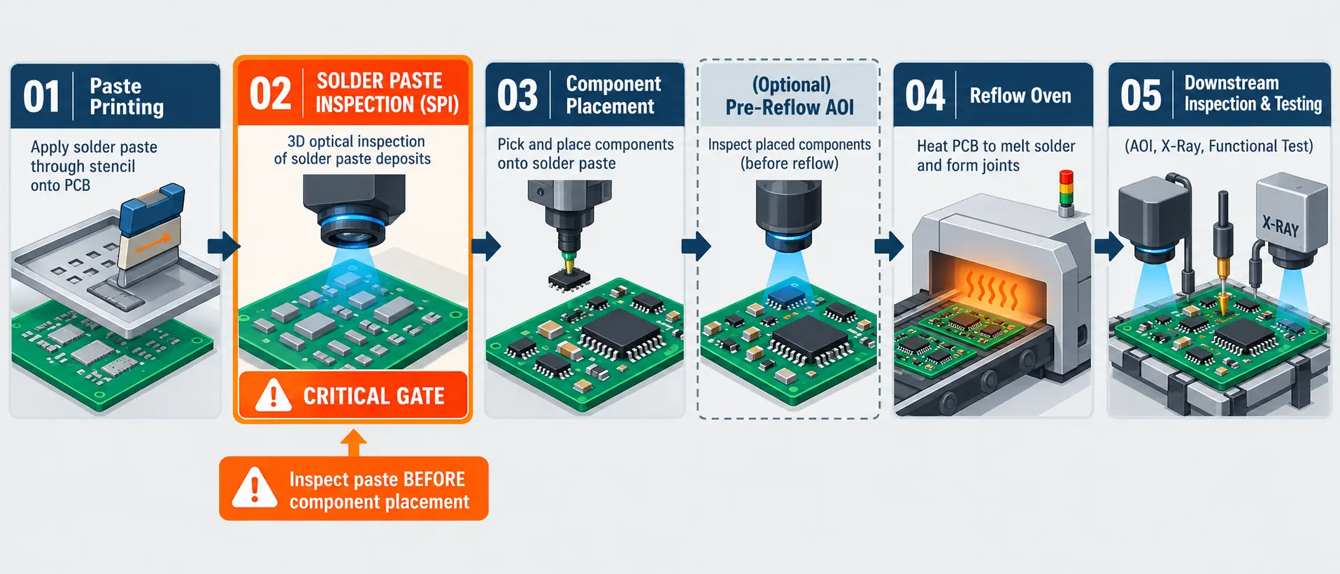
솔더 페이스트 검사(SPI)란? 측정 항목, 결함 및 품질 관리
솔더 페이스트 검사(SPI)는 인쇄 후 부품 실장 전에 PCB에 도포된 페이스트를 확인합니다. 3D SPI 시스템은 도포량, 높이, 면적 및 정렬 상태를 프로그래밍된 한계값과 비교해 측정합니다. 이를 통해 인쇄 불량을 부품 실장과 리플로우 전에 보류하고 수정할 수 있습니다. 하드웨어 엔지니어와 PCBA 구매 담당자가 핵심적으로 판단해야 할 점은…
QFN 패키지란 무엇인가요? PCB 설계 및 조립을 위한 실용 가이드
QFN packages appear in everything from power supplies and wireless modules to sensors, microcontrollers, and automotive electronics. Their small footprint, short electrical paths, and efficient heat transfer make them an attractive alternative to larger leaded packages. However, the same underside connections that save space also make QFN footprint design, soldering, and inspection less forgiving. So,…

PCB 조립용 BOM: 깔끔한 PCBA BOM 작성 방법
A BOM for PCB assembly is more than a spreadsheet of parts. It is the sourcing and assembly control document that tells a PCBA manufacturer what to buy, what to populate, what to leave off, and which substitutions are allowed. If the BOM is unclear, the RFQ stalls before production ever starts. Many PCBA RFQ…
Gerber, BOM, CPL 및 적층 구조: 각 파일의 의미
Gerber, BOM, CPL, and stackup files tell a PCB manufacturer four different things. Gerber files define the board layers. The BOM defines components. The CPL defines placement. The stackup defines layer construction, materials, copper, dielectric thickness, and impedance assumptions. Many PCBA quote delays happen before production starts. Why? The factory may have board data, but…

PCBA 견적에 필요한 파일은 무엇인가요?
A PCBA quote needs more than Gerber files. For an accurate PCB assembly quotation, send Gerber files, drill files, BOM, CPL, stackup if needed, quantity, lead-time target, and test requirements. These files tell the manufacturer what to fabricate, what to source, where to place parts, and how the finished board should be accepted. If those…


PCB DFM Checklist
A PCB DFM checklist helps engineers and buyers catch manufacturability problems before a board is quoted, fabricated, assembled, or released to production. The goal is to confirm that the supplier can build the design with the required stackup, tolerances, finish, test plan, and documentation. DFM review reduces engineering holds and helps buyers compare suppliers. If…
PCB 비아 가이드: 유형, 설계 규칙 및 선택 팁
A PCB via is a plated interconnect that lets signals, power, ground, or heat move between copper layers in a printed circuit board. Via choice affects routing density, fabrication cost, assembly yield, signal integrity, and thermal performance, so it should be part of stackup and DFM planning, not a cleanup step at the end. For…

IPC-A-610: 조립품 승인 완벽 가이드
IPC-A-610 is the acceptance standard that decides whether a finished printed circuit board assembly is good enough to ship. It is the document your contract manufacturer's inspectors work from, the one your quality team argues about, and the one your purchase order probably cites without you ever having read it. Most engineers meet IPC-A-610 the…
SMT의 의미: 표면 실장 기술 알아보기
SMT means Surface-Mount Technology: a method of attaching electronic components directly onto the surface of a printed circuit board (PCB). Rather than inserting long component leads through drilled holes, SMT uses small surface-mount components that are placed on solder-coated pads and permanently connected through controlled heating. In practical terms, SMT is what makes modern electronics…
PCBA File Requirements for Flawless Manufacturing
When preparing your printed circuit board design for assembly (PCBA), providing the right manufacturing files is the difference between a smooth product launch and a costly, delayed nightmare. While most Contract Manufacturers (CMs) will hand you a basic checklist asking for a BOM and Gerber files, modern Turnkey PCB Assembly requires far more comprehensive data…