A PCB via is a plated interconnect that lets signals, power, ground, or heat move between copper layers in a printed circuit board. Via choice affects routing density, fabrication cost, assembly yield, signal integrity, and thermal performance, so it should be part of stackup and DFM planning, not a cleanup step at the end.
PCB Via Design Takeaways
- A PCB via is a plated hole that connects copper layers in a multilayer PCB.
- Through-hole vias are the standard low-complexity option; blind, buried, and microvias support denser routing.
- Via-in-pad, thermal vias, and backdrilled vias solve specific assembly, thermal, and high-speed problems.
- Always confirm via size, aspect ratio, layer pairs, fill/cap, and backdrill notes with the PCB fabricator before release.
For many standard PCB layouts, through-hole vias are enough. For dense BGAs, HDI boards, high-speed signals, thermal pads, or compact multilayer designs, engineers may need blind vias, buried vias, microvias, via-in-pad, thermal via arrays, or backdrilled vias.
This guide explains what PCB vias are, how they work, the main PCB via types, and how to choose the right via for a design without creating unnecessary manufacturing risk. For related planning, see the internal PCB DFM checklist and PCB stackup guide.
What Is a PCB Via?
A PCB via is a plated hole used to create an electrical connection between different copper layers in a printed circuit board. Common PCB via categories include through-hole, blind, buried, microvia, via-in-pad, thermal, and backdrilled vias.
In a multilayer PCB, traces, planes, and pads are distributed across separate layers. A via lets a signal, power net, ground connection, or thermal path move vertically through the board stackup.
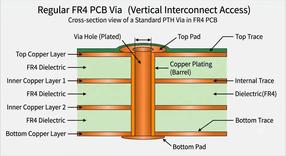
A typical via includes several basic features:
- Drilled hole: the hole created by mechanical drilling or laser drilling
- Copper barrel: the plated conductive wall inside the hole
- Via pad: the copper land around the via on connected layers
- Annular ring: the remaining copper around the drilled hole
- Antipad: the clearance opening used when the via passes through a plane it should not connect to
The simplest example is a through-hole via, which passes from the top layer to the bottom layer of the PCB. If the via barrel is plated with copper, it can connect copper features on any layer it touches. On layers where no connection is intended, the design uses clearance to keep the via isolated.
Vias are used for more than basic signal routing. PCB engineers use them to connect ground planes, route power, escape dense component packages, stitch return paths, transfer heat, and reduce routing congestion. In high-speed designs, the via structure itself can become part of the signal path, so its geometry and unused barrel length may matter.
A PCB via is different from a component through-hole. A component through-hole is designed to receive a lead, pin, connector, or mechanical feature. A via is primarily a board interconnect. Both may be drilled and plated, but their design intent is different.
The key engineering point is that a via is not just “a hole in the board.” It is an electrical, mechanical, and manufacturing feature. Its size, pad diameter, layer span, aspect ratio, plating, solder mask treatment, and location all influence whether the PCB can be built reliably and whether it will perform as intended.
How Does a PCB Via Work?
A PCB via works by turning a drilled hole into a conductive vertical path. After drilling, the hole wall is plated with copper, creating a via barrel that connects selected copper layers in a multilayer PCB.
The via does not automatically connect to every layer it passes through. It only connects to layers where the layout includes a copper pad, trace, or plane connection. On layers where the via should not connect, the PCB design creates a clearance opening around the barrel. This clearance is often called an antipad.
For example, a through-hole via may physically pass through all layers of an 8-layer PCB, but it might only connect a signal trace on layer 1 to a trace on layer 3. The remaining barrel continues through the board unless it is removed by a process such as backdrilling.
In low-speed designs, that unused barrel may not cause problems. In high-speed designs, it can act as a via stub and create signal reflections. Backdrilling is a controlled-depth drilling process used to remove unused via barrel sections in high-speed PCB designs.
The manufacturing process depends on the via type. A standard through-hole via is usually mechanically drilled through the full board after lamination, then plated. A blind via may be drilled from an outer layer to an inner layer using controlled-depth drilling or laser drilling. A buried via is formed between internal layers before final PCB lamination.
Via performance depends on several design details:
- Hole diameter and finished size
- Pad diameter and annular ring
- Copper plating thickness
- Aspect ratio
- Layer span
- Clearance to planes, traces, and pads
- Solder mask opening or tenting
- Fill, plug, or cap requirements
These details affect more than electrical continuity. A via must be manufacturable, plate reliably, survive thermal cycling, and behave properly during assembly. A via placed too close to a solder pad may draw solder away during reflow. A via with an aggressive aspect ratio may be difficult to plate.
This is why via design should be checked against the PCB manufacturer’s capabilities before release. The CAD tool can define the via, but the fabricator has to drill it, plate it, inspect it, and build it repeatedly with acceptable yield.
What Are the Main Types of PCB Vias?
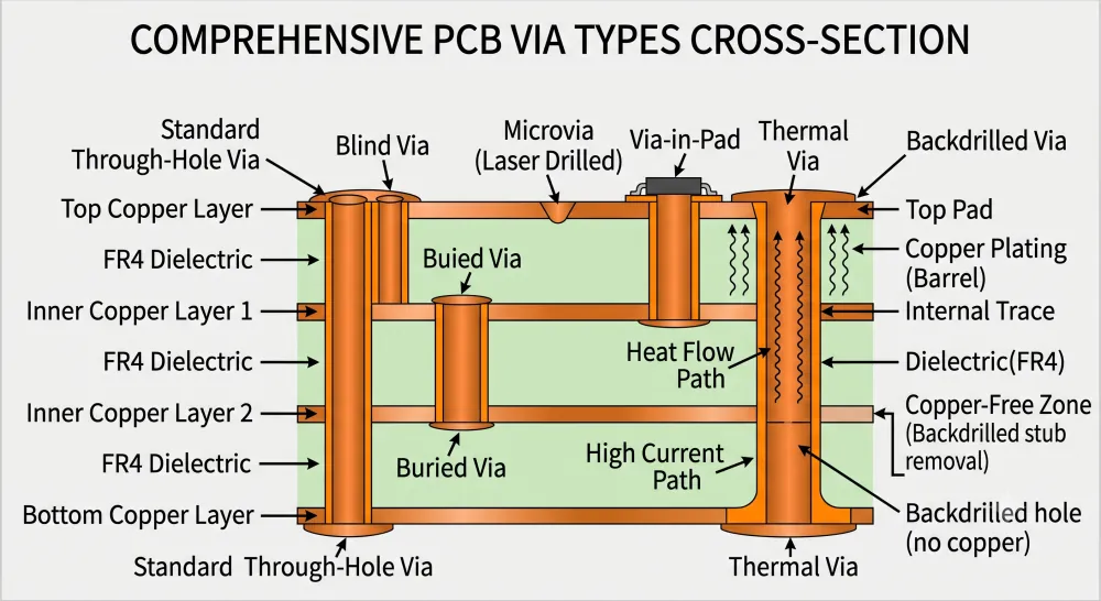
PCB vias can be grouped by the layers they connect, how they are manufactured, or the role they play in the design. Common categories include through-hole, blind, buried, microvias, stacked, staggered, tented, via-in-pad, thermal, and backdrilled vias.
For most engineering decisions, the key question is simple: which layers need to connect, and what tradeoff is acceptable in cost, routing density, performance, and reliability?
Through-Hole Vias
A through-hole via passes through the entire PCB from the top layer to the bottom layer. It is the most common PCB via type and is usually the first choice for standard multilayer designs.
Through-hole vias are popular because they are reliable, widely supported, and comparatively easy to manufacture. They are useful for general signal routing, power and ground connections, and boards where routing density is not extremely constrained.
The drawback is that a through-hole via occupies space through the full stackup. Even if it only needs to connect two layers, the drilled barrel passes through every layer. This can block routing channels and may create unused via stubs in high-speed designs.
Blind Vias
A blind via connects an outer layer to one or more internal layers without passing through the full board. It is visible from only one side of the PCB.
Blind vias are useful when engineers need more routing density near the surface of the board. They are often used for dense component fanout, HDI layouts, and designs where through-hole vias would consume too much routing space.
The tradeoff is manufacturing complexity. Blind vias require tighter process control than standard through-hole vias, and the allowed depth, diameter, and layer span depend on the fabricator’s capability. For an HDI layout, pair this decision with the HDI PCB design guide.
Buried Vias
A buried via connects only internal layers and is not visible from either outer surface. It helps free the top and bottom layers for components, sensitive signals, or additional routing.
Buried vias are useful in dense multilayer PCBs, but they usually add cost because they are created during internal layer processing before final lamination. They should be used when the routing density benefit justifies the extra fabrication steps.
Microvias
A microvia is a very small via, usually laser drilled, used in HDI PCB designs. Microvias are commonly used for short layer transitions in dense HDI boards and fine-pitch component fanout.
Because microvias use smaller pads and holes, they allow tighter routing than mechanically drilled vias. They can be blind, buried, stacked, or staggered depending on the stackup. The main tradeoff is that they require HDI fabrication capability and careful reliability review.
Via-in-Pad
Via-in-pad places a via directly inside a component pad. This technique is common under fine-pitch BGAs, high pin-count packages, and exposed thermal pads where there is not enough room to place the via outside the pad.
Via-in-pad can shorten routing paths and improve density, but it creates assembly risk if not manufactured correctly. Mechanically drilled vias in pads often require extra fabrication steps to prevent solder from wicking into the via during assembly. For assembly context, link this decision to your BGA assembly guide.
Thermal Vias
Thermal vias move heat from a component pad or copper region into internal planes, bottom-side copper, or another heat-spreading area. They are common under power ICs, voltage regulators, LEDs, and components with exposed thermal pads.
Thermal vias are often used in arrays. More vias can improve heat transfer, but the layout must also control solder behavior. Open vias in a thermal pad can draw solder away during reflow, so tenting, plugging, or filling may be needed depending on the assembly process.
Backdrilled Vias
A backdrilled via is typically a through-hole via with the unused barrel section removed by a secondary controlled-depth drilling operation. The goal is to reduce the via stub that can cause signal reflections in high-speed designs.
Backdrilling is common in high-speed digital boards, telecom equipment, networking hardware, servers, and data-center designs. It adds manufacturing cost, but it can improve signal integrity when via stubs become a performance concern. Use it alongside the high-speed PCB design checklist.
PCB Via Types Comparison Table
The best PCB via type depends on board density, stackup, component pitch, signal speed, thermal load, and cost target. Use this table as a starting point, then confirm the final structure with your PCB manufacturer.
| Via type | Layers connected | Best use case | Main advantage | Main drawback | Cost impact | When to avoid |
|---|---|---|---|---|---|---|
| Through-hole via | Top to bottom | Standard multilayer routing, power, ground | Reliable and widely supported | Uses space through the full stackup | Low | Dense HDI or high-speed channels with long stubs |
| Blind via | Outer layer to inner layer | HDI routing, BGA breakout, dense layouts | Frees routing space on unused layers | More complex fabrication | Medium to high | Cost-sensitive boards that can route with through-hole vias |
| Buried via | Inner layer to inner layer | Dense internal routing | Keeps outer layers available | Requires internal processing before final lamination | High | Simple boards or prototypes with loose density constraints |
| Microvia | Usually adjacent layers | Fine-pitch BGA, HDI boards | Supports very dense routing | Requires laser drilling and HDI process control | High | Fabricators without qualified HDI capability |
| Via-in-pad | Via placed in a component pad | BGA fanout, compact SMT layouts, thermal pads | Saves space and shortens routing path | Usually needs filling and capping | High | SMT pads where fill/cap is not specified |
| Thermal via | Heat path between copper regions | Power ICs, LEDs, voltage regulators | Improves heat spreading | Can create solder wicking risk if open | Low to high | Exposed pads without solder-control planning |
| Backdrilled via | Through-hole with stub removed | High-speed channels | Reduces reflections from via stubs | Adds controlled-depth drilling | Medium to high | Low-speed nets or designs without stub sensitivity |
A good engineering rule is to use the simplest via that satisfies the design requirement. Through-hole vias are usually the best default for standard boards. Blind vias, buried vias, and microvias are justified when routing density or layer count requires them.
Via-in-pad is useful when component pitch or thermal pad design leaves no better option. Backdrilling is worth considering when the unused via stub becomes a signal integrity concern.
How Do You Choose the Right PCB Via Type?
Choose the simplest via structure that satisfies the electrical, routing, thermal, and assembly requirement. Through-hole vias are the safest starting point. Move to blind, buried, microvia, via-in-pad, thermal via arrays, or backdrilling only when density, component pitch, heat transfer, or high-speed performance requires it.
For standard multilayer routing, start with through-hole vias. They are cost-effective, reliable, and supported by almost every PCB fabricator. If there is enough board area and enough routing space, a through-hole via is usually the safest option.
For dense component fanout, especially around BGAs, evaluate whether standard dog-bone fanout with through-hole vias will fit. If it does not, blind microvias or via-in-pad may be needed. This decision should be made together with the stackup, because BGA escape routing depends on which layers the first routing channels can reach.
For HDI designs, microvias are often the main routing tool. They allow smaller pads, tighter fanout, and short layer transitions. If multiple HDI layers are required, the design may use stacked or staggered microvias. Staggered microvias use more lateral space, while stacked microvias require tighter alignment and process control.
For high-speed signals, check the via transition as part of the signal path. A through-hole via may leave an unused barrel section that behaves like a stub. If the stub is too long for the signal speed, options include changing the routing layer, using a shorter via structure, adding ground vias near the transition, or specifying backdrilling.
For thermal design, use thermal vias to connect exposed pads or hot copper regions to larger copper planes. The via count, hole size, copper thickness, and plane connection all affect heat flow. However, assembly must be considered at the same time. Open vias in a solder pad can pull solder away during reflow, so tenting, plugging, filling, or capped via-in-pad may be required.
For cost-sensitive designs, avoid advanced vias unless they solve a specific problem. Blind vias, buried vias, filled via-in-pad, stacked microvias, and backdrilling all add process steps. Sometimes a slightly larger board, a revised placement, or a different layer count is cheaper and more reliable than forcing an aggressive via structure.
Before release, confirm three things:
- The fabricator supports the via structure.
- The dimensions match the fabricator’s design rules.
- The fabrication notes clearly specify tenting, plugging, filling, capping, or backdrilling requirements.
What PCB Via Design Rules Should Engineers Check?
PCB via design rules should come from the manufacturer’s capability table, not only from CAD defaults. The layout may pass electrical DRC and still be too small, too dense, too deep, or too poorly specified for reliable fabrication.
Start with the finished hole size. The finished hole is the final plated opening after drilling and copper plating. The drill size is usually larger than the finished hole because plating reduces the opening. If the finished size matters for current, thermal performance, test access, or fabrication notes, specify it clearly.
Next, check the via aspect ratio. Aspect ratio compares the via depth to the drilled hole diameter. A deep, narrow via is harder to plate evenly than a shallow, wider via. Through-hole vias are affected by total board thickness. Blind vias and microvias are affected by the depth of the layer span they connect.
Pad diameter and annular ring are also critical. The pad must be large enough to leave copper around the drilled hole after normal manufacturing tolerances. If the annular ring is too small, drill wander or layer misregistration can weaken the connection.
Plane clearance should not be ignored. When a via passes through a copper plane it should not connect to, the layout needs an antipad clearance. Too little clearance can create short risk. Too much clearance can disturb return current paths, especially in high-speed designs.
Spacing rules matter around dense components. Check via-to-trace, via-to-pad, and via-to-via clearance against the selected process. Minimum spacing may be acceptable in a small area, but using minimum values everywhere can reduce manufacturing yield.
Copper plating thickness affects current capacity, thermal transfer, and mechanical reliability. For high-current nets or thermal via arrays, one small via may not be enough. Designers often use multiple vias in parallel to reduce resistance and spread heat into planes.
Solder mask settings should match the assembly intent. A via near a solder pad may need tenting or plugging. A via inside a pad may need filling and capping. Do not assume the fabricator will infer this from the layout alone.
Pre-Release PCB Via Checklist
| Check | Why it matters |
|---|---|
| Finished hole size and drill size | Confirms the final plated opening matches the design intent |
| Pad diameter and annular ring | Protects against drill wander and layer registration tolerance |
| Aspect ratio | Helps avoid plating and reliability problems |
| Via-to-trace and via-to-via spacing | Reduces short risk and improves manufacturing yield |
| Plane clearance and antipad size | Prevents unintended plane connections and controls return-path disruption |
| Copper plating requirements | Supports current, thermal transfer, and barrel reliability |
| Solder mask opening, tenting, or plugging | Controls exposed copper and assembly behavior |
| Fill and cap requirements for via-in-pad | Prevents solder wicking and creates a flat solderable pad |
| Backdrill depth and remaining stub target | Documents high-speed stub-control requirements |
| Layer pairs for blind, buried, or microvias | Keeps drill files, stackup, and fabrication notes aligned |
Good via design leaves enough process margin for the board to be built repeatedly, not just once.
How Should Vias Be Tented, Plugged, Filled, or Capped?
Via covering describes how the via opening is treated during solder mask, fabrication, or assembly preparation. Common via covering choices include tented vias, untented vias, plugged vias, filled vias, and capped vias.
This is different from via type. A through-hole via, blind via, or microvia describes the layer connection. Tenting, plugging, filling, and capping describe what happens to the via opening.
A tented via is covered with solder mask. Tenting helps protect exposed copper, reduce short risk, and limit solder interaction near component pads. It works best with smaller vias; larger vias may not tent completely or consistently.
An untented via is left exposed. This can be useful for probing, debugging, test access, or some thermal applications, but exposed vias near solder pads can collect solder or flux. In dense production assemblies, untented vias should be intentional, not a default.
A plugged via has the opening closed with solder mask or another plugging material. Plugging can help prevent solder, flux, or contamination from entering the via hole. It is often useful near BGA areas, wave soldering regions, or assembly-sensitive layouts.
A filled via is filled with conductive or non-conductive material. Filled vias are commonly used when the via is inside a surface-mount pad. Without fill, solder can wick into the hole during reflow and leave an unreliable joint.
A capped via is usually a filled via with copper plating over the top, creating a flat solderable surface. This is common for via-in-pad designs under BGAs and fine-pitch SMT components.
The practical rule is simple: if the via affects soldering, specify the treatment clearly. Fabrication notes should state which vias are tented, plugged, filled, capped, or left open. Do not expect the manufacturer to infer assembly intent from the layout alone.
Recommended visual: Via protection cross-section showing untented, tented, plugged, filled, and capped vias. Alt text: “PCB via covering options showing untented, tented, plugged, filled, and capped vias.”
What PCB Via Mistakes Should You Avoid?
Most via problems come from treating vias as simple layout objects instead of manufactured structures. The via may pass DRC in the CAD tool, but still create cost, yield, assembly, or performance issues later.
One common mistake is using blind or buried vias before they are truly needed. Advanced vias can solve dense routing problems, but they also add fabrication steps. For cost-sensitive boards, first check whether placement changes, routing changes, or a different layer count can solve the problem with standard through-hole vias.
Another mistake is leaving via-in-pad structures open. If a via sits inside an SMT pad and is not filled or capped, solder can wick into the hole during reflow. This can reduce solder volume under the component and cause weak joints, opens, voids, or inconsistent assembly results.
High-speed designs often suffer when via stubs are ignored. A through-hole via used for a short layer transition may leave unused copper barrel below the signal path. At high data rates, this stub can create reflections and degrade signal quality.
Designers also sometimes push via dimensions too aggressively. Very small drills, narrow annular rings, tight spacing, and high aspect ratios may improve routing density, but they can reduce manufacturing margin. If those dimensions exceed the fabricator’s standard capability, the board may become more expensive or less reliable.
Thermal vias can create their own problems when assembly is not considered. Open vias under an exposed pad may pull solder away from the thermal pad during reflow. A thermal via array should balance heat transfer with solder control, using tenting, plugging, or filling when needed.
Before release, watch for these common issues:
- Blind or buried vias used without cost justification
- Open via-in-pad under SMT components
- Thermal vias that encourage solder wicking
- Via aspect ratio beyond fabricator limits
- Too little annular ring for reliable drilling tolerance
- High-speed via stubs left unchecked
- Missing fabrication notes for tenting, plugging, filling, capping, or backdrilling
- Different via assumptions between layout, fabrication drawing, and assembly notes
A strong via design is not always the smallest or most advanced one. It is the one that meets the electrical requirement while staying practical for fabrication and assembly.
PCB Via FAQ
What is the difference between a via and a through-hole?
A via is a PCB interconnect used to connect copper layers. A through-hole can refer to any drilled hole that passes through the board, including component holes, mounting holes, and through-hole vias. In PCB design, a through-hole via is specifically a plated via that connects layers from the top to the bottom of the board.
What are the main types of PCB vias?
The main PCB via types are through-hole vias, blind vias, buried vias, microvias, via-in-pad, thermal vias, and backdrilled vias. Through-hole vias are the most common. Blind, buried, and microvias are used when routing density is higher. Via-in-pad and thermal vias solve component fanout or heat-transfer problems.
When should I use blind or buried vias?
Use blind or buried vias when standard through-hole vias consume too much routing space or prevent a dense layout from being completed. They are common in HDI boards, fine-pitch BGA fanout, and compact multilayer designs. Because they increase fabrication complexity, they should be justified by density, layer count, or performance requirements.
Can vias be placed inside pads?
Yes, vias can be placed inside pads, but they usually need special fabrication. For SMT pads, especially BGA pads, via-in-pad structures are commonly filled and capped to create a flat solderable surface. Leaving an open via in a pad can cause solder wicking and poor solder joints.
Do PCB vias affect signal integrity?
Yes. At low speeds, via effects may be minor. At high speeds, a via can create impedance discontinuities, return-path disruption, and unused barrel stubs that cause reflections. High-speed designs may require controlled via geometry, nearby ground vias, shorter layer transitions, or backdrilling.
Conclusion
PCB vias are small features with major design consequences. The right via type depends on the board stackup, routing density, component pitch, signal speed, thermal load, manufacturing capability, and cost target.
For standard boards, through-hole vias are usually the safest starting point. For dense HDI or BGA layouts, blind vias, buried vias, microvias, or via-in-pad may be necessary. For high-speed or thermal designs, via geometry, stub length, fill method, and solder behavior deserve extra attention.
Before release, confirm the via structure, dimensions, layer pairs, and covering or filling requirements with your PCB manufacturer. A well-specified via strategy helps the board route cleanly, build reliably, and perform as intended.
