A PCB thermal hotspot map helps engineers find where heat concentrates before it becomes drift, derating, solder fatigue, or field failure. Instead of treating thermal review as a late-stage check, the map turns temperature into layout evidence: which packages, copper areas, vias, planes, and airflow routes carry the thermal load.
Key Takeaways
- A PCB thermal hotspot map shows board-level temperature distribution, not only the hottest component.
- Useful maps connect temperature patterns to layout causes: weak copper spreading, sparse thermal vias, high current density, or poor airflow.
- Simulation is best for early design comparison; IR testing is best for validating real prototypes.
- Thermal fixes should be checked against fabrication, assembly, and supplier capability before production.
For PCB engineers, the value is practical. A good map tells you where to add copper, when to use thermal vias, and whether airflow or enclosure assumptions are causing the problem.
This guide explains what a PCB thermal hotspot map is, how it is created, how to read it, and how to turn the result into layout changes.
What Is a PCB Thermal Hotspot Map?
A PCB thermal hotspot map is a visual representation of temperature distribution across a printed circuit board. It highlights localized areas where heat rises above the surrounding board temperature, helping engineers identify components, copper regions, or layout structures that may create reliability or performance risk.
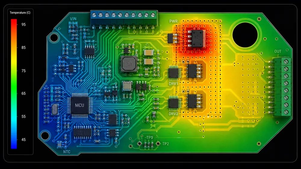
The map may come from thermal simulation software, infrared imaging, thermocouples, embedded sensors, or a combination of methods. The color palette matters less than the temperature scale and test conditions behind it.
A hotspot is not automatically a defect. Power MOSFETs, regulators, processors, LEDs, RF devices, and high-current connectors often run warmer than surrounding passives. The engineering question is whether the temperature is acceptable for the package rating, board material, solder joints, nearby components, and expected product life.
| Question | Why It Matters |
|---|---|
| Where is the highest board temperature? | Identifies the first area to investigate. |
| What generates the heat? | Separates heat sources from heat-spreading effects. |
| Where does heat stop spreading? | Points to copper, via, plane, stackup, or airflow fixes. |
| What condition produced the map? | Prevents false conclusions from unrealistic load or airflow assumptions. |
Thermal hotspot mapping should sit beside electrical and manufacturability checks. A design can pass schematic review and still fail thermally because heat has no low-resistance path into copper planes, mounting points, or airflow. If you are reviewing via strategy, the thermal role of vias connects directly with PCB via design decisions.
What Causes Thermal Hotspots on a PCB?
Thermal hotspots usually come from a mismatch between heat generation and heat removal. A component may dissipate more power than the surrounding copper, vias, planes, airflow, or enclosure can carry away.
Common causes include:
- High-power components in small areas: Regulators, MOSFETs, processors, LEDs, motor drivers, and charging ICs can create local heat when board area is limited.
- Insufficient copper spreading: A heat-generating pad connected only to a small pour, narrow trace, or isolated island will keep heat near the source.
- Weak thermal via design: Too few vias, poor via placement, or vias that do not connect to useful internal or bottom copper reduce heat transfer.
- Poor airflow or enclosure constraints: A board that works in open air may overheat inside a sealed enclosure, behind a shield, or near a battery or display.
- High current density: Narrow traces, neckdowns, connector pins, fuses, shunts, and via transitions can become heat sources because of resistive loss.
The hottest area may not be the main IC. It may be a connector, via field, shunt resistor, trace bottleneck, or copper region receiving heat from another source. Separate the heat source from the thermal bottleneck: the source generates heat, while the bottleneck prevents heat from spreading or escaping.
How Is a PCB Thermal Hotspot Map Created?
A PCB thermal hotspot map is created by modeling or measuring temperature across the board under defined operating conditions. Document load current, ambient temperature, airflow, enclosure state, duty cycle, board orientation, stackup, copper weight, and component power assumptions.
| Method | Best Used For | Main Limitation |
|---|---|---|
| Thermal simulation | Predicting risk before prototypes | Accuracy depends on model inputs |
| Infrared or sensor measurement | Validating real hardware | Surface readings can be affected by emissivity and reflections |
| Conductivity mapping | Understanding material and copper heat flow | Requires layout, image, or material processing |
Simulation-Based Thermal Maps
Thermal simulation starts with the PCB layout, stackup, copper distribution, component placement, package data, and power dissipation assumptions. The model estimates how heat spreads through copper, dielectric material, vias, solder joints, and surrounding air.
Simulation is valuable before fabrication because engineers can compare layout options while changes are still inexpensive. A designer can test thermal via arrays, copper area, copper weight, placement, and enclosure assumptions before ordering boards.
The risk is bad input data. A clean-looking simulation can be misleading if power loss, airflow, board orientation, copper thickness, enclosure temperature, or package thermal data is wrong. For power designs, model the worst credible operating condition, not only nominal load.
Measurement-Based Thermal Maps
Measurement-based maps come from real hardware. The most common method is infrared thermal imaging, often supported by thermocouples, RTDs, or embedded temperature sensors at key locations.
IR testing reveals assembly reality: solder quality, component self-heating, enclosure effects, airflow restrictions, and board-to-board variation. It can also expose unexpected heat sources, such as a connector, shunt, via transition, or copper bottleneck.
IR data still needs care. Surface readings vary with emissivity, solder mask finish, reflections, viewing angle, exposed copper, and package material. For serious validation, calibrate the setup and verify critical points with contact sensors.
For complex boards, conductivity mapping can also show how copper density, layer structure, and material choices affect heat flow. The strongest workflow combines methods: simulate early, prototype with thermal test points, measure the real board, then update the model.
How Do You Read a PCB Thermal Hotspot Map Like an Engineer?
To read a PCB thermal hotspot map correctly, start with the conditions, not the colors. A red area only has meaning when you know the ambient temperature, load profile, airflow, enclosure condition, board orientation, and temperature scale used to generate the map.
The first check is the legend. Two maps can look different even when the temperature difference is small. A 50-70°C scale can make a normal gradient look more severe than a 20-80°C scale.
Next, identify the heat source and the heat path. A tight circular hotspot suggests poor heat spreading. A long heat trail may indicate copper spreading, airflow direction, or a thermal path into a plane or mounting area.
| Map Pattern | Likely Meaning | Engineering Check |
|---|---|---|
| Small intense hotspot under one IC | High local power density or weak pad connection | Check exposed pad, copper area, and via array |
| Heat spreads along one trace or plane | Copper is carrying heat and current | Check current density and trace width |
| Hot connector or via field | Resistive loss in power path | Review pin current, via count, and plating |
| Warm zone near enclosure wall | Poor airflow or heat trapping | Check mechanical clearance and vents |
| Hot area far from main IC | Heat path, not heat source | Trace copper, plane, and mounting connections |
Compare the map against component limits. Do not judge the design only by maximum board temperature. Check junction temperature estimates, package thermal resistance, solder joint exposure, nearby component ratings, and material limits.
Also check margin. A board that passes at room temperature in open air may fail at high ambient temperature inside a sealed product.
If simulation and measurement agree on the hotspot region, the model is useful for design comparison. If they differ sharply, investigate incorrect power dissipation, missing copper details, unmodeled shields, wrong airflow, or IR measurement error.
How Can You Reduce PCB Thermal Hotspots?
You reduce PCB thermal hotspots by improving the complete heat path: from the component junction, through the package and solder joint, into copper, across layers, and into air, chassis, or another heat sink. A layout fix works only when it removes the actual bottleneck.
| Hotspot Cause | Practical Design Fix |
|---|---|
| High-power IC with small copper area | Add connected copper pour near the thermal pad |
| Heat trapped on top layer | Add thermal vias into internal or bottom copper |
| Hot high-current trace | Increase trace width, copper weight, or parallel paths |
| Hot via transition | Use more vias or larger current-carrying vias |
| Heat-sensitive part nearby | Move it away from the heat plume |
| Enclosure heat buildup | Add airflow, venting, chassis contact, or a heat spreader |
Add Connected Copper
Copper spreading is often the first PCB-level fix. Larger copper areas reduce local thermal resistance when copper connects directly to the heat source through exposed pads, short traces, wide pours, or plane connections.
Avoid isolated copper. A large pour that is thermally disconnected from the component may look helpful in layout but remove little heat. A smaller connected region often performs better than a larger floating region.
Use Thermal Vias Carefully
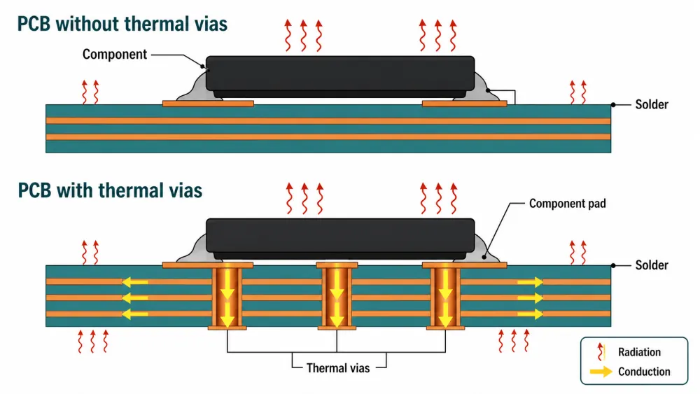
Thermal vias move heat from compact surface-mount packages into other layers. Place them close to the heat source and connect them to useful copper, planes, chassis contact, or airflow regions. For higher-power boards, review via count, drill size, plating, filling, tenting, and solder wicking risk with the PCB manufacturer.
Fix Power Paths
Some hotspots are current-density problems rather than component-cooling problems. If the hotspot follows a trace, connector, fuse, shunt, or via field, the fix may be wider traces, heavier copper, shorter paths, more vias, or better connector pin allocation.
Review Stackup and Manufacturing
If layout fixes are not enough, review stackup and mechanical heat paths. Thicker copper, additional planes, metal core substrates, thermal interface materials, chassis contact, and heatsinks can all change the hotspot pattern.
Thermal changes also need DFM review. Heavy copper, via-in-pad, filled vias, unusual stackups, and metal-backed boards can affect cost, yield, lead time, and supplier capability. Check these decisions against a PCB DFM checklist and your PCB supplier qualification checklist.
Common PCB Thermal Hotspot Mistakes
The most common mistake is treating the thermal map as a picture instead of an engineering model. If load, airflow, enclosure, stackup, and measurement assumptions are unclear, the color plot can lead to the wrong fix.
Avoid these five mistakes:
- Trusting the color scale too quickly: Always read the minimum and maximum temperatures before judging severity.
- Optimizing the wrong heat source: Trace the power path and thermal path before moving parts or adding copper.
- Ignoring worst-case conditions: Bench testing at room temperature does not represent sealed, hot, or continuous-load operation.
- Adding thermal vias without a destination: Vias need connected copper, a plane, chassis contact, or airflow region to be useful.
- Forgetting manufacturing limits: Via-in-pad, filled vias, heavy copper, and metal core boards should match supplier capability.
This is where thermal review overlaps with assembly and inspection planning. If thermal fixes change package selection, solder joints, rework access, or inspection criteria, connect the review with your PCB assembly guide and IPC-A-610 guide.
FAQ
What is a PCB thermal hotspot map used for?
A PCB thermal hotspot map finds areas of concentrated heat on a circuit board. Engineers use it to evaluate placement, copper spreading, thermal vias, airflow, enclosure effects, and high-current paths.
Is thermal simulation enough for PCB hotspot analysis?
Thermal simulation is useful for early prediction, but it should be validated with real hardware for high-power or reliability-sensitive designs. Measurement can reveal solder, airflow, enclosure, and assembly effects.
What temperature is too hot for a PCB?
There is no single safe temperature for every PCB. The limit depends on component ratings, laminate material, solder joints, ambient temperature, enclosure conditions, and expected product life.
Do thermal vias really reduce PCB hotspots?
Thermal vias reduce hotspots when they connect the heat source to useful copper, planes, or another heat removal path. They are less effective without enough vias or destination copper.
How early should thermal hotspot analysis be done?
Thermal hotspot analysis should begin during placement and stackup planning. Early review makes it easier to move hot components, reserve copper area, plan via arrays, and coordinate mechanical heat paths.
Conclusion
A PCB thermal hotspot map is most useful when it leads to a design decision. The goal is not simply to find the hottest color on the board. The goal is to understand how heat is generated, how it spreads, where it gets trapped, and which layout or mechanical change will improve the result.
For PCB engineers, the strongest workflow is straightforward: predict the risk with simulation, validate the board with measurement, compare both results, and then revise copper, vias, placement, stackup, airflow, or enclosure design. This makes thermal review part of design, not a late-stage rescue task.
Before releasing a power-dense PCB, confirm that the hotspot map uses realistic operating conditions, high-power components have connected copper and thermal vias, current paths are checked for resistive heating, sensitive components are outside sustained hot zones, and thermal fixes match fabrication capability.
For a thermal and manufacturability review, prepare the stackup, Gerbers, BOM, power dissipation table, enclosure constraints, and expected operating conditions before the design is locked.
