You have a stackup, a housing envelope, and a mechanical engineer asking for a flex PCB bend radius. The answer is not a lookup table; it is a strain calculation, and the multipliers in the tables are what that calculation returns once you fix a stackup.
Every published multiplier, whether it reads 6×, 10×, 12×, 100× or 150×, comes from IPC-2223’s minimum bend radius equations evaluated at a chosen allowable copper strain. The circulating tables detached the number from the stackup that produced it, and that is why two engineers can both follow the standard and disagree by a factor of thirty.
This article puts the stackup back: the two equations, the three strain limits, the arithmetic that links them to the published multipliers, and how to put the result on a drawing.
flex PCB types, materials and design
要点
- A bend radius multiplier is not a rule. It is what you get when you fix a stackup, choose an allowable copper strain, and solve IPC-2223’s equations.
- The standard’s own dynamic worked examples give R/T of 31 for a 185 µm single-sided stack and 88 for a 320 µm double-sided stack, not the 100× and 150× that circulate in the field.
- IPC-2223 Figure 5-7 allows rolled annealed copper under 16% deformation and electrodeposited copper under 11%. That five-point gap is why dynamic flex requires RA foil.
- The 6× static rule is roughly an order of magnitude more conservative than the standard’s own installation-bend equation, which returns an R/T near 0.55 on a thin single-sided stack.
What Is a Bend Radius on a Flex PCB?
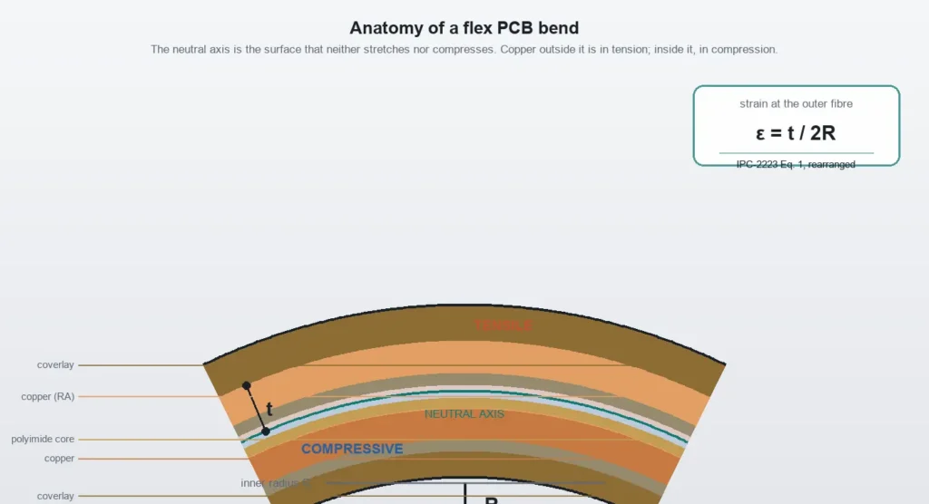
A flex PCB bend radius is the inner radius of the curved section: the distance from the innermost surface of the bent circuit to the centre of curvature.
That surface is where the calculation starts, not where the failure happens. Bend a flex circuit and the neutral axis sits somewhere inside the stack. Material outside the axis stretches; material inside it compresses. The outer foil is pulled toward its elongation limit while the inner foil buckles and delaminates from the coverlay adhesive.
The radius controls strain everywhere in the bend, and the mechanical envelope sets it. In one sentence: the radius scales with total flex thickness, scales with how far the outermost copper sits from the neutral axis, and on a fixed stack the dynamic multiplier lands close to two orders of magnitude above the static one. The standard’s own single-sided example gives R/T 31 against R/T 0.45.
How to Calculate the Minimum Bend Radius
IPC-2223 gives two equations, split by construction. Both work in micrometres.
IPC-2223 §5.2.3.4.1, single-sided with coverlay (Eq. 1):

    R = (c / 2) × [(100 - E_B) / E_B] - D

IPC-2223 §5.2.3.4.2, double-sided with coverlay (Eq. 2):

    R = (d / 2 + c) × [(100 - E_B) / E_B] - D

    R   = minimum bend radius, µm
    c   = copper thickness, µm
    d   = dielectric thickness in the flexible clad material, µm
    D   = dielectric thickness including adhesive, µm
    E_B = allowable copper deformation, %
These were read from the November 1998 base revision of IPC-2223. The current revision is IPC-2223F, dated May 2026, and the publisher’s current-revision listing is where to confirm which edition your fabricator builds to. Clause numbering has changed across revisions, so verify against a licensed copy. This article does not claim the text is identical in F.
D is subtracted because R is measured at the innermost surface, while D is the dielectric and adhesive between that surface and the copper. Thicker material under the copper puts the foil further out at the same inner radius, so a smaller R produces the same strain.
E_B takes three values: 16% for a single crease in rolled annealed copper, 10% for installation bending (flex-to-install, tied to the minimum elongation in IPC-MF-150), and 0.3% for repeated motion. Those three numbers are the only thing separating the multipliers.
Define T first. T is the sum of the base film, every copper foil, every adhesive or bondply layer, and the coverlay on both sides, measured in the bend region. It is not the nominal substrate thickness on the data sheet, and it is not the thickness at the stiffener, which is thicker by design and irrelevant to the bend. Two engineers disagreeing by a factor of two have almost always defined T differently.
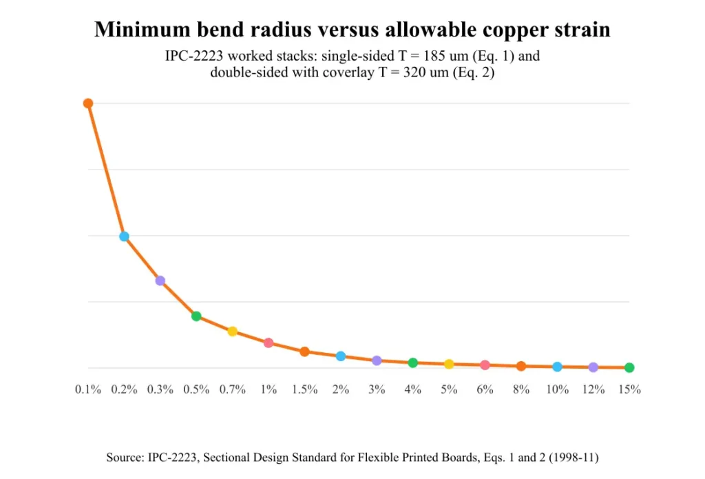
Take the standard’s single-sided example: 50 µm polyimide base, 25 µm adhesive, 35 µm copper, and coverlay with its adhesive. That is T = 185 µm, c = 35 µm, D = 75 µm. At E_B = 0.3%, Eq. 1 returns 5,741 µm, or 5.74 mm, an R/T of 31.
Take the double-sided example: a 50 µm polyimide core, two adhesive layers, two 35 µm copper foils, coverlay on both faces. That is T = 320 µm, d = 100 µm, c = 35 µm, D = 75 µm. At 0.3%, Eq. 2 returns 28,173 µm, or 28.17 mm, an R/T of 88.
Hold that stack fixed and change only the application. At the 10% installation limit, Eq. 1 returns 82.5 µm, or 0.083 mm, an R/T of 0.45. The geometry did not move; the answer moved by a factor of 69. A flex-to-install bend and a dynamic hinge are different design regimes.
That 0.083 mm is below anything you can form and inspect reliably, and the equation does not care. On a thinner stack the first term falls further, and D can exceed it, at which point Eq. 1 returns a negative radius. That is not an arithmetic error: it means the strain limit is no longer binding, because copper that thin tolerates almost any radius the process can produce. Read a negative result as “not the governing constraint” and set the drawing value from what the tooling and the coverlay will survive without creasing.
Report the diameter with the radius. A 5.74 mm radius is an 11.5 mm minimum bend diameter, and the mechanical engineer sizing the housing thinks in diameter, because that is the gap between two walls. Then add 20% to 30% for production: T varies with adhesive flow and lamination, and the formed radius carries its own tolerance. The 5.74 mm result becomes 6.9 mm to 7.5 mm.
Run the calculation on the finished stack, not the design intent. Coverlay adhesive flows during lamination, so the finished T sits a few micrometres above or below the nominal sum, and a fabricator quoting a build will give a finished thickness range rather than one number. Use the top of that range for a dynamic part. The radius scales linearly with T, so a 5% thickness overrun is a 5% radius overrun, and on a 28 mm dynamic radius that is well over a millimetre of housing nobody budgeted for.
Why the Multiplier Changes: The Strain Math
The equations are not empirical fits. They are the geometry of a bent beam written in the standard’s notation, and the rearrangement is short enough to do on a whiteboard. Bend a layer of thickness c so its inner surface has radius R. The neutral axis sits at R + c/2, the outer surface at R + c. The outer arc is longer in proportion to the radii, so strain at the outer fibre is (c/2)/(R + c/2), which reduces to c/(2R + c). Set that equal to E_B/100 and solve:
R = (c / 2) × [(100 / E_B) - 1]This is Eq. 1 with D removed. Add the dielectric offset back, because R is measured at the inner surface rather than at the copper’s inner fibre, and you have the standard’s equation exactly. The familiar relation epsilon = t/(2R), with t the distance from the neutral axis, is the same statement in approximate form: set t = c and invert, and you get (c/2)(100/E_B), which is the standard’s own expression without the small exact-form correction. The derivation belongs to IPC-2223. The point is that the equation is already the strain relation.
So a multiplier is the factor (100/E_B – 1) at a chosen strain, scaled by how far the copper sits from the axis and divided by total thickness. For the three limits that factor is 5.25, 9 and 332. Moving from 10% to 0.3% multiplies it by 37 before any geometric term changes.
The limits come from IPC-2223 Figure 5-7, which gives maximum deformation under 16% for rolled annealed copper and under 11% for electrodeposited copper. That gap answers the question designers ask most often about dynamic flex. RA foil is not preferred because of folklore about grain structure; the standard allows it roughly 45% more deformation before the copper is considered failed, and at 0.3% per cycle that margin separates a hinge that survives qualification from one that cracks.
Keep those base-foil figures separate from the plated-copper recommendations in §4.3.1.1 and §4.3.1.2, which give 12% and 18% elongation for electrolytically plated copper in through-holes, measured per IPC-TM-650 Method 2.4.18.1. They are different quantities on different features and they are not interchangeable with the RA and ED limits. A bend region contains base foil, not plated barrel, so Figure 5-7 is the figure that governs the radius.
One inconsistency is worth flagging rather than smoothing over. Figure 5-7 shows about 3% for installation bending, while the §5.2.3.4.1 worked calculation uses 10% for the same case. The two do not agree, and this article does not resolve which is intended. The 10% figure is the more permissive one, so a design built to 10% carries less margin than the number implies. Read 3% as conservative when the bend is formed once and must not crack in the field.
Layer count enters through the same lever arm. Each added layer moves copper further from the neutral axis and adds stiffness, so strain at the outermost foil rises at an unchanged radius. A 300 µm four-layer stack with 25 µm coverlay puts its outermost copper about 125 µm from the axis. At E_B = 0.3% that requires R = 41.5 mm, an R/T of 138.
非対称な接着剤ベースの積層構造では、中立軸も中央面には位置しません。接着剤はポリイミドより柔らかく、銅の分布も均一ではないため、中立軸は剛性の高い側へ移動します。最外層の銅までの距離は対称構造を前提とした計算より大きくなり、実際のひずみは形状から推測される値より高くなります。
ここからが、規格の静的曲げルールの読み方を変えるポイントです。カバーレイ25 µm、接着剤12 µm、銅18 µm、ベースフィルム25 µmの薄い片面積層構造では、T = 80 µm、c = 18 µm、D = 37 µmです。取り付け時のひずみ限界10%を式1に当てはめると、R = 81 – 37 = 44 µmとなり、R/Tは0.55です。同じ80 µmに6×ルールを適用すると480 µmになります。この半径では、外側の銅に生じるひずみは約1.9%で、許容値10%に対して、箔が耐えられるひずみのおよそ5分の1です。静的な倍率は、規格の最小値ではなく、保守的な経験則です。手作業での成形や積層のばらつきは実際にあるため、余裕が無駄というわけではありません。ただし、その余裕を選んでいることは理解しておくべきです。
自分の設計に適用する倍率
右欄は、代表的な積層構造についてIPC-2223の式から得られるR/Tであり、このページのために設定した範囲ではありません。
| 状態 | 公表されている値 | 式から得られる値 | 用途 |
|---|---|---|---|
| 静的、片面または両面、一度限りの取り付け曲げ | 6×~10× | 取り付け時のひずみ限界10%でR/T 0.45~0.55 | 公表値は保守的です。どちらでも使えますが、6×が安全側の標準値です |
| 静的、3層以上 | 12×~24× | 積層構造によって異なり、計算が必要 | 計算する |
| 動的、単層 | 100× | E_B 0.3%でR/T 31 | 185 µmの積層構造では、100×は規格独自の結果に近い値です |
| 動的、カバーレイ付き両面 | 100×~150× | 規格の320 µm積層構造ではR/T 88 | 150×は保守的な値です。薄い積層構造なら100×も妥当です |
| 動的、3層以上 | 100×、または“非推奨” | 300 µmの4層積層構造ではR/T 138 | 避けてください。非接着のフライングリード、またはリジッドフレックスへの移行部を使用してください |
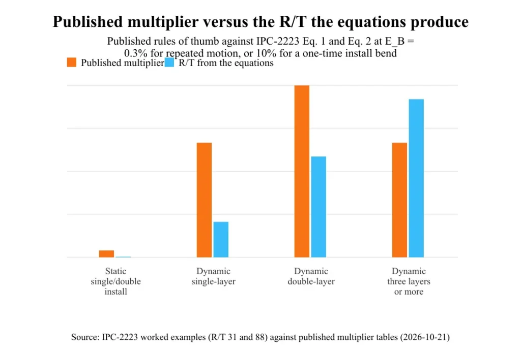
100×と150×という値には根拠がありますが、その根拠は広く知られているよりも限定的な条件に基づいています。規格の計算例では、ひずみ0.3%の場合、厚さ185 µmの片面積層構造でR/T 31、厚さ320 µmの両面積層構造で88が示されています。切りのよい数値は、これらの結果を切り上げ、元となった積層構造とは切り離したものです。100×は単層の動的曲げ条件、150×は両面層の動的曲げ条件を要約した値と考えてください。銅が2 ozの場合や4層構造の場合にも当てはまる絶対的なルールとして、どちらも扱わないでください。
判断基準:
- 一度限りの取り付け曲げ、1層または2層: 6×は安全、10×ならさらに安全です。規格では、これより小さい値も認められています。手作業で曲げる場合は、大きい方の値を使ってください。
- 一度限りの曲げ、3層以上: 計算してください。厚い積層構造や非対称な積層構造では、表は参考になりません。
- 動的曲げ、銅層1層: Tに対して100×とし、0.3%で式1を確認したうえで、必要なサイクル寿命も考慮してください。
- 動的曲げ、カバーレイ付き両面: 150×とします。ただし、積層構造が十分薄く、式からより小さい値が得られ、その値を裏付ける試験データがある場合を除きます。
- 動的曲げ、3層以上: 曲げ領域は接着しないでください。非接着のフライングリード、またはフレキシブル層を1層か2層にしたリジッドフレックスへの移行部を使用してください。
公表されている2つの見解は、これを参考にする前に訂正が必要です。
Siemensの記事「 リジッドフレックスの曲げ設計 」では、動的曲げにはフレックス材料の厚さの少なくとも10×の半径が必要だと述べています。他の公表資料はすべて少なくとも100×を示しており、規格自体の厚さ185 µmの積層構造を用いた動的曲げの例でもR/Tは31です。10×というルールは、規格の結果より一桁、業界の他の資料より一桁から二桁小さい値です。これに従うと、数回のサイクルで外側の箔に亀裂が入るヒンジになります。この数値は、静的条件または一度限りの成形条件を動的ルールとして示したものに見え、そのように受け取られるでしょう。
もう一つの訂正点は、より身近なところにあります。このサイトの一般向けフレックスPCBガイドでは、動的な片面層に20×~40×、動的な両面層に30×~50×を挙げています。これらは公表されている一般的な見解や規格の計算例より小さい値であり、大幅に短いサイクル寿命でも許容できる場合に限って使えます。自分の積層構造で実施したサイクル試験のデータが小さい半径を裏付けていない限り、大きい方の値を使ってください。以前の指針は、計算に代わる選択肢ではなく、計算によって更新されます。
出典に明記されているかどうかにかかわらず、すべての倍率には2つの条件が伴います。銅の種類(RAまたはED)と、厚さの数値に何が含まれているかです。これらを伴わない倍率は仕様値ではありません。
フレックス全体の厚さと積層構造
半径はTに比例するため、よりきつい曲げを実現するには、通常、より柔軟な材料を使うよりも積層構造を薄くするのが最も早い方法です。
| 層 | 静的フレックス | 動的フレックス |
|---|---|---|
| 銅箔 | 18 to 35 µm, RA or ED | 9 to 18 µm, RA only |
| Polyimide base film | 25 to 50 µm | 12.5 to 25 µm |
| Adhesive or bondply | Acrylic, 12 to 25 µm | Adhesiveless preferred; epoxy if bonding is required |
| カバーレイ | 25 to 50 µm per side | 25 µm per side with thin adhesive |
Standard foils are 9 µm (quarter ounce), 12 µm (third ounce), 18 µm (half ounce), 35 µm (one ounce) and 70 µm (two ounces). The 12 to 35 µm band is the production mainstream. Going to 9 µm buys a smaller radius and costs current capacity and handling robustness. Going to 70 µm for power in a bend region doubles the copper term against 35 µm, and the radius with it.
Copper type is not a preference in a dynamic build. Figure 5-7 allows RA under 16% and ED under 11%. At 0.3% per cycle you are far below both, but the gap governs how much process variation the part tolerates. Use RA for anything that moves repeatedly. For static flex, ED is acceptable and cheaper, and many fabricators default to it unless the drawing says otherwise.
Adhesive follows the same logic. Acrylic flows well and forgives lamination pressure; epoxy is stiffer and more dimensionally stable. For dynamic work the better answer is usually to remove it. An adhesiveless construction bonds copper directly to a cast polyimide film, eliminating a layer that creeps under cyclic load and cutting thickness at the same time. IPC-4204C is the material specification for the flexible metal-clad dielectrics these constructions use.
Do that trade explicitly. At a 100× multiplier, 25 µm of adhesive is 2.5 mm of radius and 5 mm of bend diameter. A designer who needs 5 mm of diameter back can often find it by deleting an adhesive layer rather than by opening the enclosure.
Keep vias out of the bend. JLCPCB’s “Flexible PCB Bend Radius: Design Guide & Rules” recommends 1.0 mm of clearance from the bend zone for static flex and 1.5 mm for dynamic. A via is a hole through the neutral axis with a copper barrel in it, and the barrel has almost no compliance in the direction the bend is pulling.
Bend Length, Tangent Length and Transition Zones
There is no published numeric minimum for the straight tangent section before or after a bend in IPC-2223. The word “straight” does not appear in the standard in this context, and “Tangent Corners” is only a figure label, not a dimensioned requirement. Anyone quoting a tangent length as an IPC value is quoting a fabricator’s practice.
The fabricator rules that do exist are useful. Eurocircuits’ guide to designing flex-to-install PCBs gives bend-zone length as L = (2π × bend radius) × (bend angle / 360), the arc length of the bend. One 180° bend at 5 mm radius consumes 15.7 mm of bend zone. The length scales with the number of bends, and that sum is often larger than the space the mechanical team allocated.
JLCPCB puts components and stiffeners at least 2.5 mm from the start of the bending region, and GCA Flex terminates stiffeners at least 1.5 mm from the bend zone start. Both make sense: a stiffener is a step change in flexural rigidity, and a bend starting at a rigidity step concentrates strain there.
Coverlay openings follow a different kind of rule. IPC-2223 §5.2.3.3 states that the circuit shall not be flexed or formed in an area where there is a discontinuity in the covercoat. That is a prohibition, not a dimension. There is no millimetre figure attached because in the standard’s model the correct distance is zero: you do not bend there. The 0.5 to 1.0 mm figures circulating from fabricators are DFM margins around that prohibition, sized to keep the bend clear of the stress concentration at an opening’s edge. They are good practice. They are not standard values, and quoting them as such invites an argument you cannot win.
The layout rule that follows is to stagger the discontinuities. The stiffener edge, the coverlay edge and the copper transition should not sit on the same plane across the bend region, so no single cross-section carries all three rigidity changes. Zoned construction is the practical version: build the bend as plain flex with coverlay both sides and no stiffener, no plated hole and no copper pour, and let the stiffeners and connectors live at the ends.
rigid-flex transition zone design]
How to Specify Bend Radius on a Fabrication Drawing
Put the number in a dedicated bend-region note or a bend table, not in the general tolerance block. A general tolerance applies to a feature the fabricator measures; a bend radius governs how the part is stacked, formed and tested.
Say which side the copper is on. A bend puts one foil in tension and the other in compression, and in a double-sided stack the outer foil is the one that cracks. If the assembly can be flipped, the drawing should say so, because a bend direction that puts the less critical copper layer outside is free margin.
Express both radius and diameter, with a tolerance. A production recommendation, not a standard value: ±0.1 mm or ±10%, whichever is greater. The percentage covers larger radii where a fixed 0.1 mm is unrealistically tight; the absolute figure covers small radii where 10% is too coarse to inspect.
The number alone is not a specification. It needs its context: the total thickness T used in the calculation, the bend angle, the direction of bend relative to the copper layers, whether the bend is static or dynamic, the target cycle count for a dynamic part, and the copper type.
A callout you can copy:
BEND REGION - SEE DETAIL B
  Minimum bend radius: 7.5 mm (diameter 15.0 mm), ±0.1 mm / ±10%
  Calculated per IPC-2223 Eq. 2 at E_B = 0.3%
  Total flex thickness T = 320 um (see stackup table)
  Bend angle: 180 deg, copper on outside of bend
  Application: DYNAMIC - 100,000 cycles, verify per IPC-TM-650 2.4.3
  Copper: rolled annealed (RA), 35 um
  Keep vias and stiffeners >= 1.5 mm from bend zone boundary
How Bend Radius Is Verified
A specified radius is a claim about endurance, and endurance is demonstrated by test rather than by geometry. The method is IPC-TM-650 Method 2.4.3, “Flexural Endurance, Flexible Printed Board Materials”, which determines the number of flexes to conductor failure. It originates with the Flexible Circuits Test Methods Subcommittee (D-15).
Be careful with the failure criterion. The method as published counts flexes to conductor failure, meaning an electrical open. Several vendor pages attribute a “10% resistance increase” criterion to it. That is a common misattribution. If resistance-rise criteria apply on your programme, they come from the applicable specification or drawing.
The method does not fix the test conditions either. Bend radius, stroke, cycle rate and specimen geometry for a given part are set by the applicable specification and drawing. A page publishing a universal cycle count for “a flex PCB” is describing its own test.
IPC-6013, the qualification and performance specification for flexible and rigid-flexible printed boards, is where flex endurance qualification is required, with the cycle count and bend radius specified by the applicable use category and performance class in the contract or drawing. Vendor sources that publish a cycle-count table attributed to IPC-6013 contradict each other and none cites a clause, so this article does not reproduce one.
Finally, IPC-A-600 is an acceptability and inspection standard, not a design standard. It defines defects such as conductor cracking and delamination in the bend area, and an inspector can reject a part against it, but it prescribes no geometric minimums. Using IPC-A-600 to answer “what radius do I need” is a category error.
IPC-A-600 acceptance criteria]
よくある質問
What is the minimum bend radius for a flex PCB?
It is calculated from your stackup, not looked up. For a one-time installation bend, Eq. 1 at the 10% limit returns an R/T near 0.45 to 0.55 on a thin single-sided stack, so 6× is a safe practical figure. For repeated motion at 0.3%, the standard’s own worked examples give R/T 31 for a 185 µm single-layer stack and 88 for a 320 µm double-layer stack with coverlay.
What is the minimum bend radius for a double-sided flex PCB?
IPC-2223’s worked example for a 320 µm double-sided stack with coverlay gives R/T 88 for dynamic flex at 0.3% strain, which is 28.17 mm, and R/T 2.15 for a one-time installation bend at 10%, which is 0.69 mm. Both assume rolled annealed copper. With ED foil the allowable deformation drops from under 16% to under 11%, and the margin goes with it.
Can a multilayer flex PCB be used for dynamic bending?
Not with the bend region bonded. A 300 µm four-layer stack puts its outermost copper about 125 µm from the neutral axis, and at 0.3% strain that requires a 41.5 mm radius, an R/T of 138. That will not fit most products, and thinning the stack far enough to fit it defeats the reason for four layers. Route unbonded flying leads across the hinge, or put the bend in a rigid-flex transition with one or two flex layers.
フレックスPCBは何回曲げられますか?
サイクル寿命は材料ではなく設計の特性であり、表から引用するものではなく、試験によって確認します。IPC-TM-650 Method 2.4.3では導体が破損するまでの屈曲回数を測定します。試験条件と合格回数は、適用される仕様書および図面で定めます。積層構成、曲げ半径、試験条件が示されていない公表サイクル数は、設計の入力値にはなりません。
温度によって曲げ半径は変わりますか?
はい。銅の伸びと接着剤の弾性率はどちらも動作温度範囲によって変化するため、20 °Cで安全な曲げ半径でも、温度範囲の上限では余裕が小さくなります。接着剤を使用した構造は、接着剤が軟化してクリープするため、接着剤を使用しない構造より影響を受けやすくなります。最悪条件となる使用温度を想定して指定してください。電源段の近くにある部品では、その温度はラベルに記載された周囲温度とは異なります。
曲げ半径と曲げ直径の違いは何ですか?
半径は曲率の中心から内側の表面までの距離です。直径はその2倍で、曲げ全体を横切って測ります。半径5 mmは直径10 mmです。「曲げ5 mm」とだけ書かれた図面は、どちらを指すのか不明確です。両方を指定してください。隙間の寸法を決める機械設計者は直径で考え、設計式では半径を使います。
まとめ
設計ガイドにある倍率は、積層構成を考慮しないひずみ計算に基づいています。積層構成を計算に戻しましょう。曲げ領域の厚さTを合計し、用途に応じたひずみ限度(RA銅の単一折り目では16%、取り付け時では10%、繰り返し動作では0.3%)を選んで、式1または式2を適用します。その後、20%~30%の余裕を加え、半径と直径を併記してください。銅の種類、曲げ方向、サイクル数とともに、両方を図面に記載します。
設計上の制約内に収まらない場合、通常は注記の数値を小さくするのではなく、積層を薄くするか、曲げ部分の層数を減らすのが解決策です。