Reflow soldering is the process that attaches surface-mount components to a printed circuit board by heating stencilled solder paste until it melts, wets the component terminations and forms the joint on cooling. It is the primary assembly method for almost every modern electronic product, and it is the step where the most expensive mistakes become permanent.
Most technical guides stop at the oven. They explain the four zones, list the usual defects and finish with a sales page. What they rarely explain is the part that actually decides yield: the profile is built per assembly rather than per oven, the numbers on a paste data sheet and the numbers in a components standard serve different purposes, and a joint is only “good” relative to a named acceptance class.
This guide covers the process from print to inspection, the parameters that govern it, how to validate a profile on a mixed-mass board, and how the common defects map to acceptance criteria rather than to an inspector’s opinion.
要点
- The reflow profile is set per assembly, not per oven. Board thickness, copper mass and component mix change how heat arrives, so the same recipe that passes on one product can underheat another.
- Time above liquidus is the parameter that governs joint quality in both directions. Too little leaves incomplete wetting; too much grows an intermetallic layer thick enough to embrittle the joint.
- Published reflow limits differ because they answer different questions. A paste data sheet describes the profile you should run; IPC/JEDEC J-STD-020 describes the worst case a component must survive.
- Most defects are set before the oven. Tombstoning, bridging and warpage trace back to pad symmetry, aperture design and copper balance – layout and stencil decisions no profile can fully offset.
- Lead-free joints are supposed to look dull. Judging a SAC305 joint against the shine of a tin-lead joint is the most common inspection error in the field.
What Is Reflow Soldering?
Reflow soldering is a process in which solder paste, stencilled onto the pads of a printed circuit board, is heated until it melts, wets the component terminations and forms the electrical and mechanical joint on cooling.
The name is literal. The solder arrives as a paste of metal powder suspended in flux, and the joint is formed when that paste reflows: it liquefies, coalesces and solidifies in place. Nothing is fed into the joint during the process. The correct amount of solder was already on the board, or it never will be.
That distinction is what made reflow the default method for surface-mount assembly. Every joint on the board forms in a single thermal cycle, so component count stops being a cost driver in the way it was for hand and wave soldering. Fine-pitch packages, dense boards and double-sided assemblies all become practical when one pass through an oven can join thousands of points at once.
It is worth separating reflow from wave soldering early, because the two are frequently confused. In reflow, solder paste applied to the pads melts where it sits. In wave soldering, the board is passed over a standing wave of molten solder so that solder wicks up through plated holes. Wave remains the high-volume answer for through-hole content; reflow is the answer for surface-mount. Most production boards use both.
This guide is written for the people who have to make the process hold: process engineers qualifying a line, NPI engineers taking a new product to production, quality engineers deciding what to accept, and design engineers whose layout decisions arrive at the printer before anyone else sees them.
How the Reflow Process Works, Step by Step
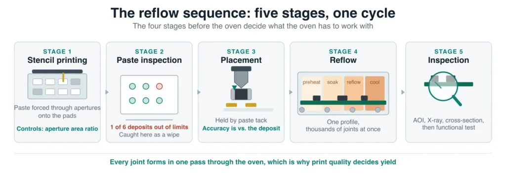
Reflow soldering is five stages, and the four that happen before the oven decide whether the oven has anything to work with.
1. Stencil printing. A laser-cut stainless steel stencil is aligned to the board, and a squeegee drives paste through the apertures onto the pads. The controlling geometry is the area ratio: the area of the aperture opening divided by the area of its walls. If that ratio is too low, paste adheres to the aperture wall more strongly than to the pad and stays in the stencil instead of transferring. A pad can be starved of solder before the board has moved.
2. Solder paste inspection. An SPI system measures the volume, area, height and alignment of every deposit against limits. This is the cheapest defect gate on the line and the one most often skipped on prototype builds. A print defect caught here costs a wipe. The same defect caught after reflow costs a rework: the part is removed, the site is cleaned and re-pasted, and the joint and the surrounding laminate take another thermal cycle. The gap between those two outcomes is the whole argument for keeping SPI in the line.
3. Component placement. Pick-and-place machines place parts onto the wet paste, which holds them by tack and surface tension until the oven. Placement accuracy is usually quoted by the machine vendor at a stated sigma and component size, but what actually matters is placement relative to the paste deposit. A well-placed part on a misprinted pad is a defect waiting for heat.
4. Reflow. The board is carried through a multi-zone oven and subjected to a controlled temperature profile. The paste melts, the flux activates and burns off its work, the alloy wets the pad and the termination, and the assembly is cooled at a controlled rate. The next two sections take this apart.
5. Inspection. Automated optical inspection checks what can be seen; X-ray checks what cannot; cross-section settles disputes; functional test confirms the product works. Each answers a different question, and the acceptance section explains which one settles the argument.
The Reflow Profile, Zone by Zone
A reflow profile is the temperature the assembly experiences plotted against time. It is set per assembly rather than per oven, because board thickness, layer count, copper distribution and component thermal mass all change how quickly heat reaches a given joint.
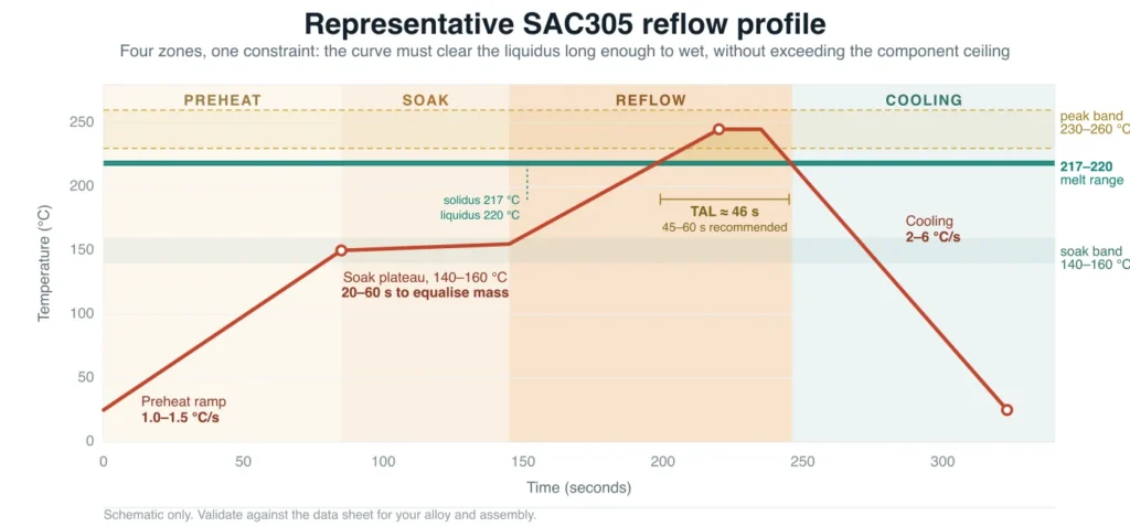
A typical profile has four zones. Each has a purpose, a window, and a specific failure mode when it is wrong.
Preheat
The board is brought from ambient to the soak temperature at a controlled ramp. Its ramp rate exists to limit thermal shock: heating too fast cracks ceramic capacitors and multilayer ceramics, and it spatters the paste, which is where stray solder balls come from. Solvents and volatiles in the paste begin to leave the deposit here.
Indium Corporation’s published reflow limits for SAC305 paste specify an average ramp of 1.0 to 1.5 °C/s, with 0.5 to 2.5 °C/s acceptable (Indium Corporation, SAC305 water-soluble paste data sheet、取得日:2026年10月21日)。
Soak
The soak holds the assembly in a temperature band so that everything reaches thermal equilibrium before the peak. This is its real job. Components of different mass heat at different rates, and without a plateau the heavy parts arrive at the peak late while the light parts are already past it.
Soak is also where flux does its chemistry: it reduces the oxides on the pad and the termination so the alloy can wet them. Run the soak too long or too hot and the flux is consumed before the alloy melts. The result shows up as graping, where the solder particles fail to coalesce into a single mass, and as head-in-pillow, where a BGA ball and its paste never merge.
Reflow
The assembly is taken above the alloy’s liquidus so the solder melts, wets both surfaces and forms the metallurgical bond. What governs here is time above liquidus, usually abbreviated TAL: the number of seconds the joint spends molten.
TAL is a two-sided constraint. Too little time and the alloy does not fully wet the pad and the termination, which produces a weak or intermittent joint. Too much time and the intermetallic layer between the solder and the copper grows thicker than it needs to be, which leaves the joint more brittle than the bulk alloy predicts. Separately, the peak is capped by what the components can survive.
Indium’s SAC305 data sheets specify 45 to 60 seconds above liquidus as recommended, with 30 to 100 seconds acceptable, and a peak of 230 to 260 °C. SAC305 is not a true eutectic: it melts over a narrow range, with a solidus of 217 °C and a liquidus of 220 °C (Indium Corporation, alloy data for Indalloy 256, retrieved 2026-10-21). Both windows are anchored to the liquidus rather than chosen in isolation. The peak band sits 10 to 40 °C above it – the floor set by the alloy, the ceiling by what the components will survive – while the TAL window is the time the alloy spends above that line.
Cooling
Cooling solidifies the joint and sets its grain structure. It is the most neglected zone on the profile, and the one where two legitimate concerns pull against each other.
Indium’s data sheets recommend 2 to 6 °C/s with 0.5 to 6 °C/s acceptable, noting that faster cooling promotes a finer grain structure. The opposing concern is thermal stress. Ceramic capacitors and the laminate itself are damaged by a steep temperature gradient, which is why some assemblers cap the cooling slope well below the paste window’s upper bound. Both effects are real. Cool too slowly and the grain coarsens while intermetallic growth continues; cool too fast and the parts and laminate take a shock they were not qualified for.
There is no universal number that resolves it. The paste data sheet sets the window the alloy tolerates. The component data sheet sets the gradient the package tolerates. The assembly’s thermal mass sets what the oven can physically deliver. Where those conflict, the component limit governs, because that is where the damage is irreversible.
RSS vs RTS: Choosing a Profile Shape
Two profile shapes cover most production work, and the choice is governed by how uneven the thermal mass on the board is.
| 特性 | Ramp-soak-spike (RSS) | Ramp-to-spike (RTS) |
|---|---|---|
| Shape | Ramp, plateau, spike, cool | Continuous ramp, peak, cool |
| Thermal uniformity | High, because the plateau equalises | Lower, because light parts lead |
| Process time | Longer | Shorter |
| 最適な用途 | Mixed thermal mass, dense assemblies, large boards | Simple boards with uniform mass |
| Main risk | Flux exhaustion if the soak runs long | Cold joints on heavy parts, voiding |
RSS holds the assembly at a plateau so that heavy and light components arrive at the peak together. RTS removes the plateau and runs a single ramp, which is faster and consumes oven time efficiently but leaves more thermal spread across the board.
Most production assemblies with a genuinely mixed component mix end up on a soak profile. If a board carries both a 01005 passive and a large power inductor, the plateau is what stops one from being overfired while the other is underfired.
How to Build and Validate a Reflow Profile
Build the profile from the paste data sheet, not from the oven’s saved recipe. The paste defines the window; the oven is adjusted to fit inside it. Validation then proves that the assembly, not just the paste, stays in that window.
1. Read the constraints off the data sheet. Ramp rate, soak band and duration, peak range, TAL and maximum peak temperature. These are the limits. Everything that follows is adjustment within them.
2. Set the component ceiling. The lowest maximum body temperature among the parts on the board caps the peak, and reflow classification for moisture-sensitive packages is defined in IPC/JEDEC J-STD-020. A profile that satisfies the paste but exceeds a component’s classification temperature is still wrong, and the failure may not appear until the product is in the field.
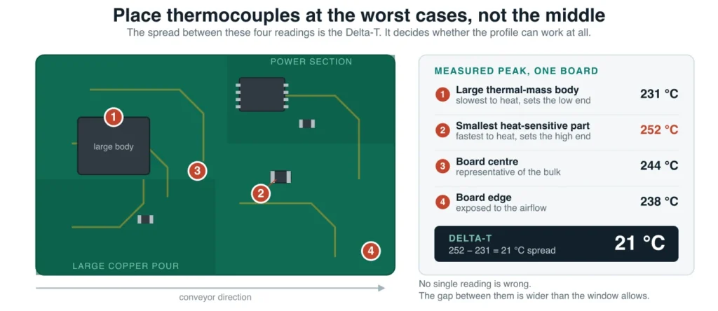
3. Attach thermocouples to the worst cases, not to the middle. Place them on the largest thermal mass component, the smallest and most heat-sensitive part, the centre of the board, and the board edge. Add one under a BGA where it can be done. The centre-to-edge spread of these readings is the Delta-T, and it is the single number that tells you whether the profile is viable.
4. Run the profile and read the Delta-T. If the spread across the board exceeds what the process window allows, the profile is not yet finished regardless of whether each individual thermocouple looks acceptable.
5. Close the Delta-T gap in a fixed order. Conveyor speed first, because it shifts the whole curve in time without changing zone relationships. Then zone setpoints, which change the shape. Then zone boundaries, and only if the first two cannot close it. Changing several at once makes the result uninterpretable.
6. Record and control it. Store the profile against board revision, paste lot and date. Re-profile when the paste changes, the stackup changes, the component mix changes, after oven maintenance or repair, and on a periodic interval as part of process control. A profile you cannot reproduce is not a control; it is a coincidence.
The Delta-T problem is the one that catches NPI engineers, and it is worth stating plainly. On a board with a small, dense logic section and a large ground-poured power section, the two areas can run tens of degrees apart through the peak. You cannot fix that by raising the peak, because the light area was already at its limit. You fix it by slowing the ramp, extending the soak so the heavy area catches up, or changing the board: adding thermal relief, balancing copper, or moving the heavy components together.
Reflow Temperatures by Solder Alloy
The reflow window follows the alloy’s liquidus temperature. The peak is set far enough above liquidus to guarantee complete melting and wetting, and no further than the components will tolerate.
| Alloy | Composition | Solidus / liquidus | Typical peak | 一般的な液相線温度以上時間(TAL) | 注記 |
|---|---|---|---|---|---|
| SAC305 | Sn 96.5 / Ag 3.0 / Cu 0.5 | 217 / 220 °C | 230~260 °C | 推奨:45~60秒 | 鉛フリー作業の量産基準 |
| Sn63/Pb37 | Sn 63 / Pb 37 | 183 °C(共晶) | 約210~220 °C | 30~60秒 | より広いプロセスウィンドウ。ただし、RoHS適用除外の場合に限り使用可能 |
| Sn42/Bi58 | Sn 42 / Bi 58 | 138 °C(共晶) | 約165~180 °C | ペーストのデータシートを参照 | 熱に弱い部品および2回目のリフロー向け |
この表では、数値そのものよりも重要な点が2つあります。
J-STD-020とペーストのデータシートは、同じ内容を説明しているわけではありません。 IPC/JEDEC J-STD-020は、プラスチック製表面実装パッケージの吸湿感度分類を定めています。Pbフリー試験プロファイルでは、150~200 °Cで60~120秒のソーク、217 °Cを超える温度で60~150秒の保持、さらに最大260 °Cの分類ピーク温度が規定されています。これは、部品がベンチ上で複数回のサイクルにわたって耐えることを求められる最悪条件です。基板で実行することを推奨する条件ではありません。この2つを混同すると、エンジニアはペーストに必要な条件よりもはるかに高温かつ長時間のプロファイルを設定してしまいます。
異種合金を混在させたアセンブリは、材料の細かな違いではなく、プロセス上の判断事項です。 基板の鉛含有表面仕上げに鉛フリーペーストを使う場合、またはその逆の場合、接合部の界面における組成が変化します。その結果は許容できる場合もありますが、在庫品を偶然使った結果ではなく、根拠を示したうえで文書化された判断であるべきです。
従来の錫鉛はんだの使用が合法であるのは、有害物質使用制限指令(2011/65/EU)に基づく適用除外の範囲内に限られます。同指令は、公表された適用除外リストの対象となる場合を除き、電気・電子機器中の鉛を制限しています(欧州委員会、RoHS指令、2026-10-21閲覧)。ご使用の製品に適用除外が適用されると決めつけず、最新のリストを確認してください。
はんだペーストの選定と取り扱い
はんだペーストは、金属粉末をフラックスと媒体の系に分散させたものです。粉末の粒径タイプは、好みや価格ではなく、基板上で最も狭いピッチに基づいて選びます。
粉末の粒径。 IPC J-STD-005では、粒子の一定割合が公称範囲内に入ることに基づいて、はんだ粉末を分類しています。より細かい粉末は微細な開口部への印刷に適していますが、単位質量あたりの表面酸化物が多く、ボイドが発生しやすく、ステンシル寿命も短くなります。基本的には、基板上で最も狭いピッチに対応できる範囲で、最も粗いタイプを選びます。
| 粉末タイプ | 粒径範囲 | 一般的な用途 | トレードオフ |
|---|---|---|---|
| タイプ3 | 25~45 µm | 標準ピッチ、0.5 mm以上 | ステンシル寿命が最長で、ボイドが最少 |
| タイプ4 | 20~38 µm | ファインピッチ、約0.4~0.5 mm | バランスがよく、ファインピッチで一般的な選択肢 |
| タイプ5 | 15~25 µm | 極細ピッチ、0.3 mm以下 | 最も微細な印刷が可能だが、酸化物負荷が最大で、寿命が最短 |
フラックスの化学特性。 ノークリーン、水溶性、ロジン系のフラックスは、活性度と残渣がそれぞれ異なります。選択は印刷工程で行いますが、その影響が現れるのは後工程です。コンフォーマルコーティング、清浄度試験、あるいは部品の下に残った残渣が原因と判明する現場故障などがその例です。アセンブリにコーティングを施す場合は、ペーストの認定後ではなく、その前にコーティング材のサプライヤーに適合性を確認してください。
金属含有率と粘度 ペーストが開口部をどのように通過するか、またステンシル上でどれだけの時間使用可能かを左右します。これらは印刷品質を左右する変数であり、一定の値ではありません。温度やステンシル上に置かれている時間によって変化します。
保管と取り扱い。 はんだペーストは通常、冷蔵保管され、使用前に室温に戻す必要があります。冷たいペーストを印刷すると水分が結露し、印刷が不均一になるためです。ステンシル上での使用可能時間には上限があり、メーカーが指定しています。長時間開封したままのペーストは、未開封時とは異なる印刷結果になり、その違いは堆積量のばらつきとして現れます。SPIで検出されますが、誰もその結果を信じようとしないでしょう。
リフロー装置と仕様の決め方
市場を分ける加熱技術は3種類あります。どれを選ぶかは、どれが最新かではなく、均一性、熱容量への対応力、コストの兼ね合いで決まります。
強制対流、赤外線、気相リフロー
強制対流 は、生産現場で標準的に使われる方式です。複数の独立制御ゾーンで加熱した空気を循環させ、基板上に空気を直接吹き付けることで、部品の色、材質、仕上げにかかわらず、露出したすべての表面に対流で熱を伝えます。そのため、部品が混在する基板でも均一に加熱できます。ゾーン数は加熱プロファイルの分解能を示す仕様であり、品質を示すものではありません。ゾーンが多いほどプロファイルを細かく設定できますが、はんだ接合部の品質が向上するわけではありません。
赤外線 加熱は、放射によってエネルギーを伝えます。効率がよく、機械的な構造もシンプルですが、材質によってエネルギーの吸収率が異なり、影になる部分では大型部品がその背後の領域を遮ってしまうことがあります。このため、現在では生産ラインよりも卓上型やリワーク用の装置で一般的に使われています。
気相リフロー では、組立品を不活性な過フッ素化液体の飽和蒸気に浸します。蒸気が基板上で凝縮し、液体の沸点で決まる一定温度で潜熱を伝えます。熱伝達が非常に均一なため、熱容量の大きい部品や熱に弱い部品に適しています。また、蒸気が酸素を置換するため、酸化が抑えられます。一方で、液体のコストや取り扱いに加え、多くのシステムでは連続工程ではなくバッチ処理となる点がトレードオフです。
窒素と真空
窒素による不活性化は、リフロー中の酸化を抑え、ぬれ性を向上させます。特に、ファインピッチのパッケージ、鉛フリー合金、高信頼性製品で重要です。窒素はランニングコストがかかるため、欠陥の低減によってその費用を回収できるかどうかで判断します。単純な基板を製造する、成熟した適切に管理されたラインでは、費用に見合わないことが少なくありません。一方、自動車用や医療用製品のファインピッチBGAやQFNの製造では、多くの場合、費用に見合います。
真空リフローでは、合金が溶融している間に真空をかけ、接合部に閉じ込められたガスを引き抜いて、ボイドを大幅に減らします。下面端子型パッケージやアレイパッケージのボイドを減らすうえで、最も効果的な手段です。これはプロファイルの調整ではなく、設備投資に関する判断です。
必要な生産能力に合わせた炉のサイズ選定
炉のサイズ選定の計算例
ある実装業者は、1時間あたり180枚の基板を生産する必要があります。各基板の長さは8インチで、はんだペーストメーカーが推奨するプロファイルは、3段階で4分間です。基板間に2インチの間隔を設けるコンベヤーを使用するため、負荷率は0.8です。
ステップ1。1分あたりの基板枚数。 180 ÷ 60 = 1分あたり3枚。
ステップ2。必要なライン速度。 (3枚/分 × 8インチ/枚)÷ 0.8 = 毎分30インチ.
ステップ3。必要な加熱長。 毎分30インチ × 4分 = 120インチ、つまり10フィート.
炉には少なくとも120インチの 加熱 長さが必要です。冷却部、投入部、排出部は加熱ゾーンの外側にあるため、炉全体の長さはこれより長くなります。加熱長ではなく全長を基準に見積もるのは、よくある誤解であり、コストにも大きく影響します。
リフローに適した基板設計
リフロー不良の多くは、基板が印刷機に到達する前の設計段階で作り込まれています。チップ立ち、ブリッジ、反りは、それぞれ特定のレイアウトやステンシルの選択に起因します。
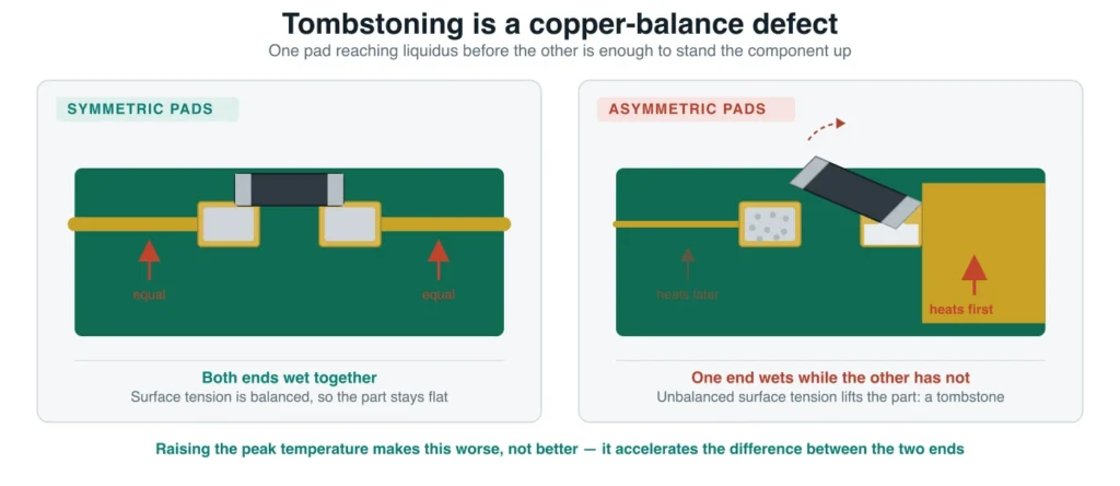
部品の両端のパッド間における熱的な対称性 が、チップ立ちの発生を左右します。一方のパッドが大きな銅箔につながり、もう一方が細い配線につながっていると、部品の片端がもう一方より先に液相線温度に達します。先に達した側がぬれ、表面張力で引っ張られて部品が立ち上がります。両端の銅箔のバランスを整えれば、この欠陥はほぼ解消します。
パネル全体の銅箔バランス は反りを左右します。大きな銅箔領域の分布が不均衡だと、加熱と膨張にむらが生じ、ピーク温度を通過する際にパネルが反ります。対策として、基板そのものではなく、パネルの捨て代に銅箔を追加し、分布を均等にします。
コンベヤーの進行方向に対する部品の向き は、長い部品の場合に重要です。細長い部品を気流と同じ向きではなく、気流を横切る向きに配置すると、合金が溶融している間に部品が持ち上がったり、ずれたりする可能性を低減できます。
パッドの形状と間隔 はブリッジの発生を左右します。はんだブリッジは、炉ではなくペースト量と間隔の問題です。プロファイルではなく、ステンシルを調整して対処します。
エッジレールとキープアウト領域 は、コンベヤーが基板を固定するための箇所となり、搬送中に基板端部の部品やペーストが乱されるのを防ぎます。
パッケージごとのステンシル開口部の設計ルール が、残りの課題の多くを解決します。
- ファインピッチ部品では、応力集中を減らし、ペーストの抜け性を高めるため、開口部の端を丸くします。
- BGAパッドや超小型受動部品では、堆積量を均一にし、予測どおりのはんだボールを形成するため、四角い開口部を使います。
- QFNのサーマルパッドでは、大きな露出パッドの下に供給するペースト量を調整し、端部のはんだビーディングを減らすため、十字形の開口部を使います。
- ファインピッチ部品では、間隔ではなく過剰なペースト量がブリッジの原因となるため、開口部を縮小します。
フィデューシャルマーク は、マウンターに信頼性の高い基準点を与えます。これがないと、実装精度はマウンターではなく、基板の製造公差やパネル位置合わせの精度によって制限されます。
穴埋めなしのパッド・オン・ビア リフロー中にペーストがバレル内へ吸い込まれ、接合部のはんだが不足し、反対側まで汚染されます。ビアをパッド内に配置する必要がある場合は、樹脂などで充填してキャップ処理を行い、充填タイプをIPC-4761に基づいて指定してください。 プリント基板ビア構造の保護に関する設計ガイドでは、ビアの保護タイプとその受け入れ基準が定義されています。これは基板を発注する前に決定しておくべき製造上の事項です。
両面実装および混載技術による組み立て
実際の製品の多くは、すべてが表面実装部品というわけではありません。スルーホール部品をどう扱うか、また両面実装をどの順序で行うかは、新しい組み立て案件ごとに検討が必要です。
2回目のリフロー
両面基板では、まず片面をリフローし、基板を反転させてから、もう一方の面にペーストを印刷し、部品を搭載してリフローします。問題は、最初の面のはんだ接合部が2回目の熱サイクルにさらされ、合金が固相線温度を超えると軟化することです。
実用上のルールは、工程順序と部品の質量に集約されます。部品が少ない、または小さい側を先に実装し、重い部品は2回目の工程に回して、落下の危険を避けます。重い部品を先に実装する必要がある場合は、接着剤を点付けして2回目のリフロー中も固定します。通常、2回目の工程ではピーク温度をやや低く設定し、設計によっては基板裏面をサーマルシールドで保護します。
リフローラインでのスルーホール部品の実装
混載実装では、通常、次の3つの方法のいずれかが使われます。
| 工程 | 適した基板構成 | 生産量の目安 | 主な制約 |
|---|---|---|---|
| ピン・イン・ペースト | それ以外がSMT部品で構成された基板へのスルーホール部品の実装 | 少量から大量まで | はんだペーストで接合部だけでなくバレル内も満たす必要があるため、開口部を大きくし、ペーストの塗布量を増やす必要があります |
| 選択はんだ付け | スルーホール部品が比較的少ない混載基板 | 少量から中量 | ノズルのアクセス性と接合部ごとのサイクル時間 |
| フローはんだ付け | スルーホール専用基板または混載基板 | 大量 | SMT面を保護するマスキングまたは治具 |
ピン・イン・ペーストは工程を丸ごと一つ省けるため、理解しておく価値が最も高い方法です。スルーホールパッド上に、バレル内を満たしながらフィレットも形成できるだけのペースト量を確保するため、開口部を広げて印刷します。その後、部品を搭載し、組み立て全体を一度にリフローします。制約となるのはペースト量です。接合部とバレルの両方を満たす必要があるため、表面実装部品用の同じパッドと比べて、開口部を大きくし、ペーストの堆積を厚くしなければなりません。
判断の基準は、部品構成と生産量です。工程の選択は好みではなく、スルーホール部品の数によって決まります。同じ基板の組み立てに複数の工程を使うケースがほとんどです。そうでないかのように扱うと、見積もりを誤ることになります。
よくあるリフロー不良とその原因
リフロー不良は偶然に起きるものではありません。よくある不良には、それぞれ限られた原因があり、その原因は測定可能な工程パラメーターか、検査可能なレイアウト上の選択に関係しています。
| 不良 | 外観 | 主な原因 | 対策 | 受け入れクラス |
|---|---|---|---|---|
| マンハッタン現象 | チップ部品の片端が持ち上がり、垂直に立つ | パッド間の熱的不均衡、ペースト量の不均一、または昇温速度が速すぎること | パッドの銅箔を均衡させ、ペーストの塗布量をそろえ、昇温速度を下げる | クラス2およびクラス3:端子がパッドから完全に浮いている場合は不合格 |
| ブリッジ | はんだが隣接するパッドまたはリード同士を接続している | ペースト量の過剰、開口部の設計、ステンシルの密着不良 | 開口部を小さくし、印刷圧力を調整して、位置合わせを確認する | クラス2およびクラス3:導体間の短絡となるブリッジは不合格 |
| ボイド | 接合部内部の気泡。BGA、QFN、パワー系パッケージで特によく見られる | ガス放出、酸化、ペーストの取り扱い、昇温速度 | ボイド低減タイプのペーストを使用し、予熱時間を延ばし、真空または窒素の使用を検討する | クラス3はより厳格です。該当する基準および合意済みのボイド許容限度に照らして評価してください |
| ヘッド・イン・ピロー | BGAボールがペースト上に載っているが、合金化していない | リフロー時のパッケージまたは基板の反り。酸化によって悪化する | ペースト量を増やし、耐酸化性の高いフラックスを使用し、プロファイルを調整して、不活性雰囲気にする | クラス3:接合部が金属学的に形成されていないため不合格 |
| グレーピング | ブドウの房のような、粒状で酸化した表面 | 過度のソークまたはTALにより、合金化する前にフラックスが消耗した | ソークを短縮し、TALを短縮して、より熱安定性の高いペーストを使用する | ぬれ不足のため不合格 |
| はんだボールの発生 | パッドや配線の周囲に散在する小さな球状物 | 昇温が速すぎること、ステンシルの洗浄不良、または劣化したペーストによるペーストの飛散 | 予熱をゆっくり行い、ステンシルを洗浄し、ペーストの使用期限を管理する | サイズと位置によるため、該当する基準に照らして評価する |
| 低温接合または接合部の乱れ | 艶のない、粗い、または破断したフィレット | ピーク温度またはTALの不足、あるいは溶融中の振動 | ペーストのデータシートに照らしてプロファイルを確認し、コンベヤーを安定させる | ぬれ不足のため不合格 |
| 部品のずれまたは傾き | リフロー中に部品がパッドからずれた状態 | ぬれの不均衡、コンベヤーの振動、または気流の乱れ | ペースト量のバランスを取り、搬送を安定させ、ファンの設定を見直す | 実装基準に照らして評価する |
| 反り | ピーク温度に達する間に基板またはパネルが反る | 銅箔の不均衡、非対称な積層構成、湿気 | 銅箔のバランスを取り、積層構成を見直し、リフロー前にベーキングする | 接合部の状態によって、工程指標または欠陥となる |
| ポップコーン現象 | 吸収された水分がピーク温度で急激に気化することによる、亀裂または層間剥離 | 吸湿性パッケージがリフロー前に吸収した水分 | IPC/JEDEC J-STD-033のスケジュールに従ってベーキングし、フロアライフを管理する | 欠陥:パッケージが損傷している |
ボイドとヘッド・イン・ピローは、見た目上形成されている接合部は実際にも形成されている、という同じ前提を覆します。トゥームストーニングがこの一覧に含まれるのは、別の理由からです。目視できる欠陥ですが、不均衡はパッドの銅箔パターンに組み込まれているため、昇温を遅くすれば発生を抑えられる場合はあるものの、根本的な解決にはレイアウトまたはステンシルの変更が必要です。
アレイパッケージのボイド は、プロファイル変更の効果が最も小さい欠陥です。合金が凝固する前にガスが抜けきらないとボイドが形成されるため、調整すべき要素は昇温速度、ペーストの化学組成、予熱時間、雰囲気です。BGAやQFNではガスの排出経路が長いため、ガルウィング部品よりもボイドが発生しやすくなります。最も効果の高い単独の対策は真空リフローです。より低コストな対策としては、低ボイドペーストの使用や、より長く穏やかな予熱が挙げられます。
ヘッド・イン・ピロー は、上から見ると接合部が形成されているように見えるため、検査で最も見逃されやすい欠陥です。その発生メカニズムは反りです。リフロー中に反ったパッケージがボールをペーストから浮かせ、再び平らになる頃にはペーストがボールに接合しないままリフローを終えています。Indium Corporationのこの欠陥に関する技術資料では、その原因はリフロー時の部品または基板の反りであり、酸化によって悪化すると説明されています。また、最も実用的な対策としてはんだペーストを推奨しています(Indium Corporation, ヘッド・イン・ピローの検査と予防, 2026-10-21閲覧)。検出には通常、X線検査または染色・剥離試験が必要です。そのため、BGA基板の初品評価には、いずれかの検査を含めるべきです。
マンハッタン現象 は、設計段階で作り込まれる欠陥の最も明確な例です。公表されている対策は、パッドの対称性とペースト量の一貫性を保つことで、どちらもレイアウトとステンシルの設計に関わります。「確実にぬれさせる」ためにピーク温度を上げると、トゥームストーニングは改善するどころか悪化します。両端の差が拡大するためです。
検査および合否判定基準
検査では、工程が適切に機能したかを確認します。合否判定では、結果が許容できる品質かどうかを判断します。これは別々の問いであり、異なる規格に基づいて判定されます。
工程順に、確認項目は次のとおりです。 SPI リフロー前:ペースト量と位置合わせを確認する。 AOI リフロー後:部品の有無、極性、位置合わせ、および目視可能な接合部の形状を確認する。 X線検査 目視できない接合部について。実際には、BGA、QFN、その他の底面端子部品が対象です。 断面観察 X線検査で判定が難しく、重大な問題が疑われる場合の破壊検査に、そして 機能試験に 最終製品レベルの判定基準として用います。
受入判定は別の階層です。接合部は検査員の目視ではなく、明確に指定された規格とクラスに基づいて評価します。その規格はIPC-A-610、 電子組立品の許容基準で、現在の版は2024年発行のリビジョンJであり、リビジョンHに代わるものです。判定基準は製品クラスごとに定められており、クラス1は一般電子機器、クラス2は専用サービス電子機器、クラス3は高性能製品および過酷な環境で使用される製品を対象とします。
実務上、次の2つの帰結があります。
クラスは生産開始前に決める商業上の判断であり、作業台で下す評価ではありません。 使用環境上必要のない製品にクラス3を選ぶと、信頼性は向上しないまま検査コストだけが増えます。車両内で熱サイクルにさらされる製品にクラス2を選ぶと、保証上の問題を招きます。
鉛フリーはんだ接合部は、異なる外観になるのが普通です。 SAC305のフィレットは通常、光沢のある凹形の鉛入りはんだフィレットよりも光沢が鈍く、粒状で、丸みを帯びています。鉛フリー接合部を光沢で判定するのは旧来の基準であり、誤った不合格判定を招くだけでなく、実際に欠陥のある接合部がたまたま光沢を帯びている場合に、誤った安心感を生むことにもなります。
この規格の各判定基準には、「許容可能」「工程指標」「欠陥」という3つの状態があります。最も議論になりやすいのは中間の状態です。「工程指標」とは、理想的ではないものの、指定されたクラスにおける形状、適合性、機能を損なわない状態であり、基板を不合格にする理由にはなりません。工程指標をすべて欠陥として扱うと、元の状態よりも大きなリスクをもたらす手直しが増えます。また、クラス3製品では、仕様が求めていないコストまで増加します。
リフロー工程の認定方法
リフロー工程の認定とは、生産開始前に工程が管理状態にあることを文書で証明することです。提出物は初品記録であり、見栄えのよい基板ではありません。
- プロファイルの取得。 すべての熱電対の測定値とデルタTを記載した初品プロファイルの記録。
- はんだペーストのトレーサビリティ。 合金、ロット、粉末タイプ、日付を、使用したプロファイルに紐づけて記録。
- SPIの限度値。 この特定の組立品に対する体積と位置合わせの限度値を設定し、文書化。
- AOIの検査範囲。 デフォルト設定のままにせず、この組立品で実際に発生する欠陥に合わせてプログラムを調整。
- 隠れた接合部。 アレイパッケージの初品検査を含む、X線検査のサンプリング計画を策定。
- 記録。 基板のリビジョン、はんだペーストのロット、日付に紐づけてプロファイルを保存。
- プロファイル再取得の契機。 文書化し、責任者となる役割を明確に指定。
- 受入クラス。 規格番号とリビジョン記号を明記して文書に記録。
- 手直し。 手直し後の接合部をどのように再検査するかも含め、判定基準と許容される手直し回数を定義。
- 湿気に対する感受性。 対象部品を特定し、ベーキングとフロアライフの管理を実施。
よくある質問
フローはんだ付けとリフローはんだ付けの違いは何ですか?
リフローはんだ付けでは、パッドに塗布されたペースト状のはんだが、塗布された場所で溶融します。フローはんだ付け(ウェーブはんだ付け)では、溶融はんだの波に基板を通し、はんだがめっきスルーホールを通って上がります。リフローは表面実装部品に、ウェーブはスルーホール部品に用いられ、多くの量産基板では両方の工程が使われます。
ヒートガンではんだをリフローできますか?
単一部品の取り外しや交換には使えますが、基板の組み立てには使えません。ヒートガンには制御された昇温、ソーク、測定可能なピーク温度がないため、温度プロファイルを実現できず、再現性のある接合部も作れません。これは手直し用の工具ですが、手直しに使う場合でも、積層板の剥離や周辺部品の過熱を招くおそれがあります。
自宅ではんだをリフローするにはどうすればよいですか?
現実的な方法は、ホットプレート、改造したトースターオーブン、またはホットエアステーションを使うことです。いずれもゾーン制御や測定済みのプロファイルを実現できないため、液相線温度を超える時間やピーク温度を検証できず、接合されたように見えるかどうか以上の受入基準もありません。安全上重要でない基板の試作であれば、妥当な割り切りと言えます。しかし、管理された工程の代わりにはなりません。
タイプ4のはんだペーストとは何ですか?
タイプ4は、IPC J-STD-005における粉末粒径の分類で、粒径範囲は20~38 µmです。0.4~0.5 mm程度のファインピッチ作業で一般的に選ばれます。基板上の最小ピッチに対応できる範囲で、できるだけ粗いタイプを選んでください。粉末が細かいほど印刷性は向上しますが、酸化が速くなり、ステンシルの寿命が短くなるためです。
リフローはんだ付けの理想的な温度は何度ですか?
ピーク温度は合金によって決まり、部品の耐熱温度によって上限が定まるため、単一の温度はありません。217~220 °Cで溶融するSAC305の場合、推奨される液相線温度超過時間は45~60秒で、公表されているピーク温度の範囲は230~260 °Cです。上限は、基板上の部品のうち、最高温度の許容値が最も低いものによって決まります。
鉛フリーはんだの接合部が鈍く見えるのはなぜですか?
SAC305の接合部は通常、光沢が鈍く粒状だからです。多くの検査員が良好な接合部の特徴と考える、光沢のある凹形のフィレットは、鉛入りはんだ合金に特有のものです。鉛フリー接合部を光沢で判定するのは旧来の基準であり、鉛フリー組立品の検査で最もよくある誤りです。
リフロープロファイルはどのくらいの頻度で再検証すべきですか?
はんだペースト、積層構成、部品構成が変わったとき、またはオーブンの保守や修理を行ったときには、必ずプロファイルを再取得してください。また、工程管理の一環として、定期的にも実施してください。基板のリビジョンに紐づけて保存されていても、はんだペーストのロットに紐づいていないプロファイルは記録として不完全です。はんだペーストを変更するだけでも結果が変わることがあるためです。
まず確認すること
何かを変更する前に、自分の工程について2点確認してください。第一に、実際に製造している組立品に基づいてプロファイルを検証したのか、それとも類似基板のプロファイルを流用したのか。第二に、受入クラスが規格のリビジョンとともに文書化されているのか、それとも暗黙の了解になっているのか。
プロファイルが引き継がれたものであれば、最も手早く改善する方法は、通常、新しいオーブン設定ではありません。現行の基板でDelta-Tを測定することです。これにより、そのプロファイルが実装品全体で機能し得るものかどうかが分かります。クラスが推定されているのであれば、最も低コストな改善策は、次回の発注書にクラスを明記することです。費用はかからず、そうしなければ最終検査時に持ち上がる議論を避けられます。
どちらの確認もほとんど費用がかからず、尋ねればサプライヤーが直接回答してくれる内容です。プロファイルについて尋ねた場合は、熱電対の波形と基板のリビジョンが記載されたチャートが提示されるはずです。クラスについて尋ねた場合は、名称、リビジョン記号、日付が提示されるはずです。それより曖昧な回答は、未確認として扱うのが妥当です。
参考資料
- Indium Corporation, SAC305水溶性はんだペーストの製品データシート。推奨および許容される昇温速度、ソーク時間の範囲、液相線温度以上の時間、ピーク温度、冷却速度を参照。取得日:2026-10-21。
- Indium Corporation, Indalloy 256 (SAC305)のはんだ合金データ。固相線温度217 °C、液相線温度220 °Cを参照。取得日:2026-10-21。
- Indium Corporation, ヘッド・イン・ピローの検査と予防。ヘッド・イン・ピローの反りおよび酸化のメカニズムと、推奨される対策に関する技術論文。取得日:2026-10-21。
- IPC / Global Electronics Association、 規格に適合する。IPC-A-610、J-STD-001および関連規格群の適用範囲を参照。取得日:2026-10-21。
- IPC、 IPC-A-610J:電子組立品の受入基準。2024年発行。2020年のRevision Hに代わる版。IPCおよび認定販売代理店から入手可能。以下を含む ANSI Webstore.
- IPC/JEDEC、 J-STD-020:非気密封止ソリッドステート表面実装デバイスの耐湿性/リフロー感度分類。鉛フリー分類プロファイルの限界値および分類時のピーク温度を参照。
- IPC、 J-STD-005:はんだペーストの要求事項。タイプ3(25~45 µm)、タイプ4(20~38 µm)、タイプ5(15~25 µm)を含む、はんだ粉末の粒径分類を参照。
- IPC/JEDEC、 J-STD-033:耐湿性/リフロー感度表面実装デバイスの取り扱い、梱包、輸送および使用。耐湿性に関する項で参照されているベーク条件およびフロアライフ管理を参照。
- IPC、 IPC-4761:プリント基板ビア構造の保護に関する設計ガイド。基板設計に関する項で参照されているビア保護タイプを参照。
- 欧州委員会、 RoHS指令。電気・電子機器における鉛の使用制限および適用除外の仕組みを参照。取得日:2026-10-21。