PCB実装
ここでは、PCB設計から組み立てまでの全工程に関する専門知識に加え、エレクトロニクス業界の最新動向を的確に分析する知識を身につけられます。
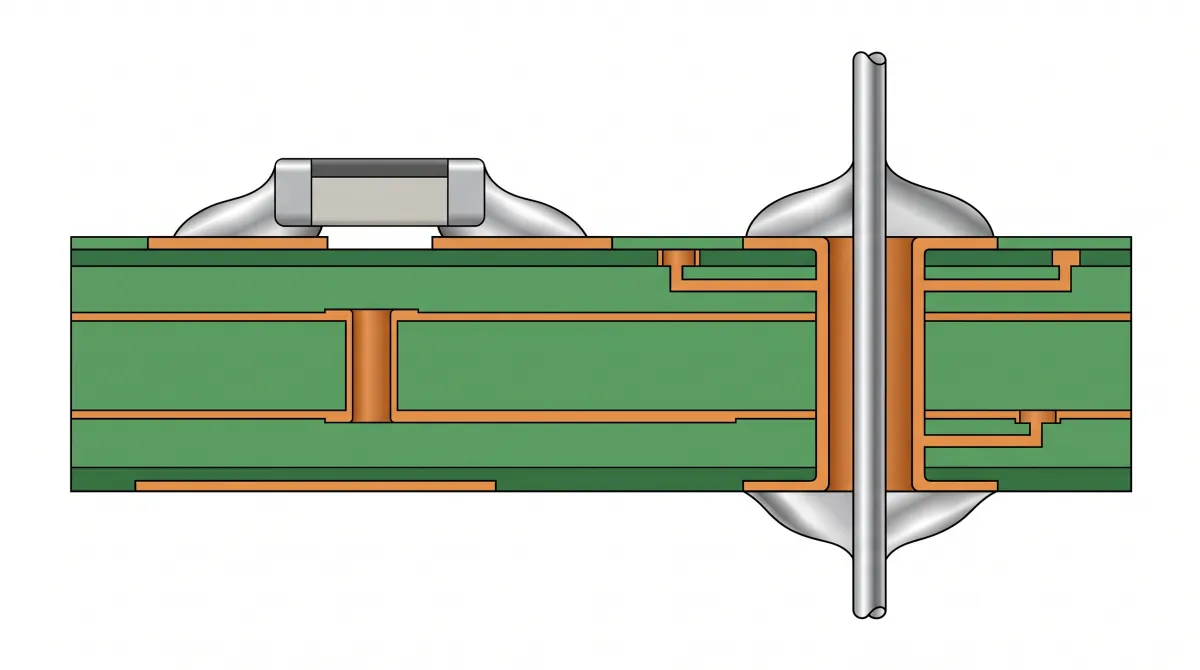
表面実装とスルーホールの比較:主な違い、コスト、選び方
Surface-mount components attach to pads on a circuit board's surface. Through-hole components have leads that pass into holes in the board for soldering. Surface-mount technology (SMT) often suits compact layouts and automated assembly; through-hole technology (THT) can be useful when a selected component or its mechanical load calls for it. Many boards use both. The…
PCBとPCBAの違いとは?
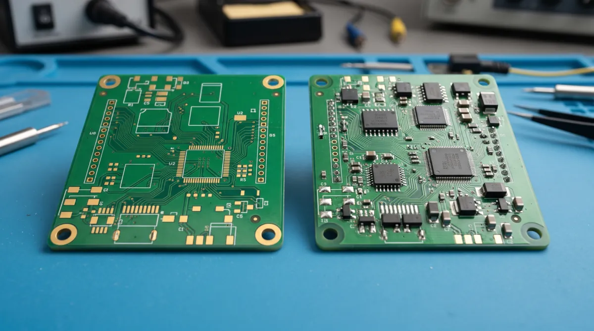
PCB vs PCBA comes down to the deliverable: in a manufacturing order, a PCB commonly means a bare printed circuit board, while PCBA can mean the assembly process or the board after components have been mounted. A populated board is not automatically programmed, functionally tested, or ready to install in a finished product. The terms…
PCB用はんだフラックス:種類、用途、洗浄方法
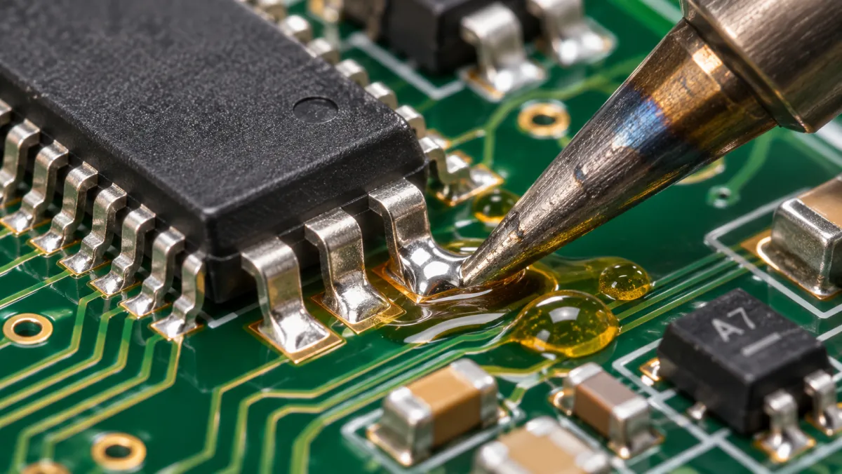
はんだフラックスは、酸化物を除去し、加熱中に酸化が再び起こるのを抑えることで、はんだが金属表面になじみやすくなるようにする化学組成物です。プリント基板の組み立てでは、単独で塗布するほか、はんだ線やはんだペーストに含まれている場合もあります。フラックスの選択は、接合部の形成だけでなく、…に残る残渣にも影響します。
IPC J-STD-001:はんだ付け要求事項ガイド
IPC J-STD-001「Requirements for Soldered Electrical and Electronic Assemblies(はんだ付けされた電気・電子アセンブリの要求事項)」は、はんだ付けアセンブリに使用する材料、工程、および合否判定の要求事項を定めています。アセンブリの製造方法に加え、完成した接続部に対する要求事項も対象です。この規格を指定する発注書には、適用する改訂版、製品クラス、プロジェクト固有の要求事項を明記してください。アセンブリの購入担当者にとって、…
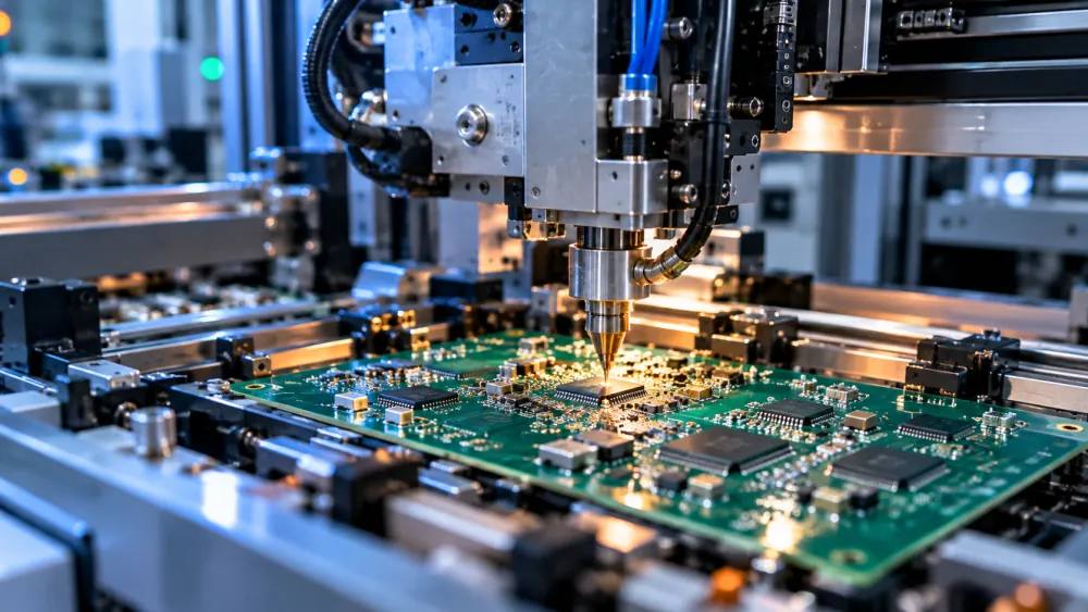
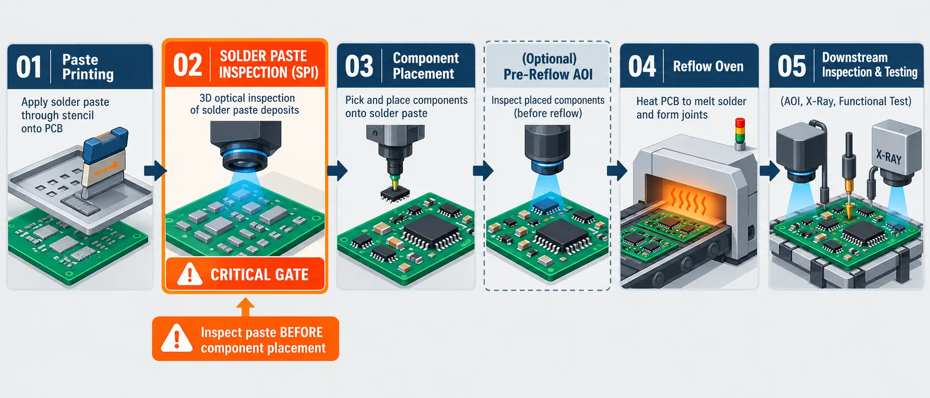
はんだペースト検査(SPI)とは?測定項目、不具合、品質管理
はんだペースト検査(SPI)では、印刷後、部品を搭載する前のPCB上のはんだペーストを確認します。3D SPIシステムは、堆積したペーストの体積、高さ、面積、位置合わせを、設定済みの許容範囲と照合します。不良印刷を部品搭載やリフローの前に保留し、修正できるようになります。ハードウェアエンジニアやPCBAの購入担当者にとって重要なのは、…
QFNパッケージとは?PCB設計・実装の実践ガイド
QFN packages appear in everything from power supplies and wireless modules to sensors, microcontrollers, and automotive electronics. Their small footprint, short electrical paths, and efficient heat transfer make them an attractive alternative to larger leaded packages. However, the same underside connections that save space also make QFN footprint design, soldering, and inspection less forgiving. So,…

PCB実装向けBOM:明確なPCBA用BOMの作成方法
A BOM for PCB assembly is more than a spreadsheet of parts. It is the sourcing and assembly control document that tells a PCBA manufacturer what to buy, what to populate, what to leave off, and which substitutions are allowed. If the BOM is unclear, the RFQ stalls before production ever starts. Many PCBA RFQ…
ガーバー、BOM、CPL、スタックアップ:各ファイルの意味
Gerber, BOM, CPL, and stackup files tell a PCB manufacturer four different things. Gerber files define the board layers. The BOM defines components. The CPL defines placement. The stackup defines layer construction, materials, copper, dielectric thickness, and impedance assumptions. Many PCBA quote delays happen before production starts. Why? The factory may have board data, but…

PCBAの見積もりにはどのファイルが必要ですか?
A PCBA quote needs more than Gerber files. For an accurate PCB assembly quotation, send Gerber files, drill files, BOM, CPL, stackup if needed, quantity, lead-time target, and test requirements. These files tell the manufacturer what to fabricate, what to source, where to place parts, and how the finished board should be accepted. If those…


PCB DFM Checklist
A PCB DFM checklist helps engineers and buyers catch manufacturability problems before a board is quoted, fabricated, assembled, or released to production. The goal is to confirm that the supplier can build the design with the required stackup, tolerances, finish, test plan, and documentation. DFM review reduces engineering holds and helps buyers compare suppliers. If…
PCBビアガイド:種類、設計ルール、選び方のヒント
A PCB via is a plated interconnect that lets signals, power, ground, or heat move between copper layers in a printed circuit board. Via choice affects routing density, fabrication cost, assembly yield, signal integrity, and thermal performance, so it should be part of stackup and DFM planning, not a cleanup step at the end. For…

IPC-A-610:実装受入れの完全ガイド
IPC-A-610 is the acceptance standard that decides whether a finished printed circuit board assembly is good enough to ship. It is the document your contract manufacturer's inspectors work from, the one your quality team argues about, and the one your purchase order probably cites without you ever having read it. Most engineers meet IPC-A-610 the…
SMTとは:表面実装技術をわかりやすく解説
SMT means Surface-Mount Technology: a method of attaching electronic components directly onto the surface of a printed circuit board (PCB). Rather than inserting long component leads through drilled holes, SMT uses small surface-mount components that are placed on solder-coated pads and permanently connected through controlled heating. In practical terms, SMT is what makes modern electronics…
PCBA File Requirements for Flawless Manufacturing
When preparing your printed circuit board design for assembly (PCBA), providing the right manufacturing files is the difference between a smooth product launch and a costly, delayed nightmare. While most Contract Manufacturers (CMs) will hand you a basic checklist asking for a BOM and Gerber files, modern Turnkey PCB Assembly requires far more comprehensive data…