電子回路
ここでは、PCB設計から組み立てまでの全工程に関する専門知識に加え、エレクトロニクス業界の最新動向を的確に分析する知識を身につけられます。
AOIとは?PCBの自動光学検査について
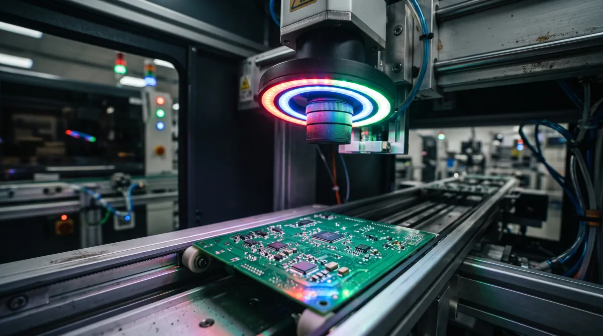
AOIとは何でしょうか。自動光学検査では、カメラ、照明、ソフトウェアを使って、回路基板に指定された目視可能な特徴や不具合の可能性を検査します。PCB組み立てでは、部品の欠落や、露出したはんだブリッジを検出できます。AOIはベアボードの銅箔パターンも検査できますが、すべての隠れた接合部を確認したり、基板が動作することを保証したりはできません。…
ドローンに使われる基板の種類とそれぞれの役割
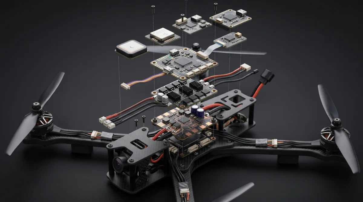
ドローンに使われる回路基板には、フライトコントローラー、電子速度コントローラー、電源分配基板、センサー・航法基板、通信基板、カメラなどのペイロード用基板があります。複数の機能を1つのアセンブリにまとめるドローンもあれば、個別のモジュールを接続するものもあります。それぞれの機能によって、プリント基板(PCB)に求められる要件は異なります。…
IPC J-STD-001:はんだ付け要求事項ガイド
IPC J-STD-001「Requirements for Soldered Electrical and Electronic Assemblies(はんだ付けされた電気・電子アセンブリの要求事項)」は、はんだ付けアセンブリに使用する材料、工程、および合否判定の要求事項を定めています。アセンブリの製造方法に加え、完成した接続部に対する要求事項も対象です。この規格を指定する発注書には、適用する改訂版、製品クラス、プロジェクト固有の要求事項を明記してください。アセンブリの購入担当者にとって、…
産業用PCB製造:工程と品質保証
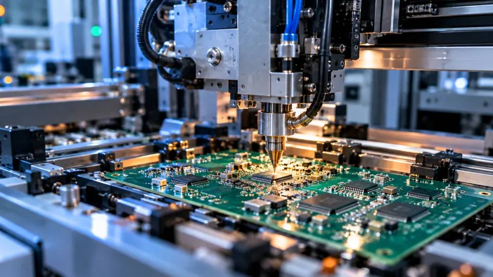
産業用PCB製造では、承認済みの回路基板設計を、ベアボードや、注文に応じて部品を実装したアセンブリへと仕上げます。製造、部品実装、検査、合意した試験を経て完成します。承認の可否は、指定された製造仕様、動作条件、合否判定基準によって決まります。モーターコントローラー、センサーインターフェース、制御盤に取り付ける制御基板では、材料や機械的な支持方法…に異なる要件が求められる場合があります。
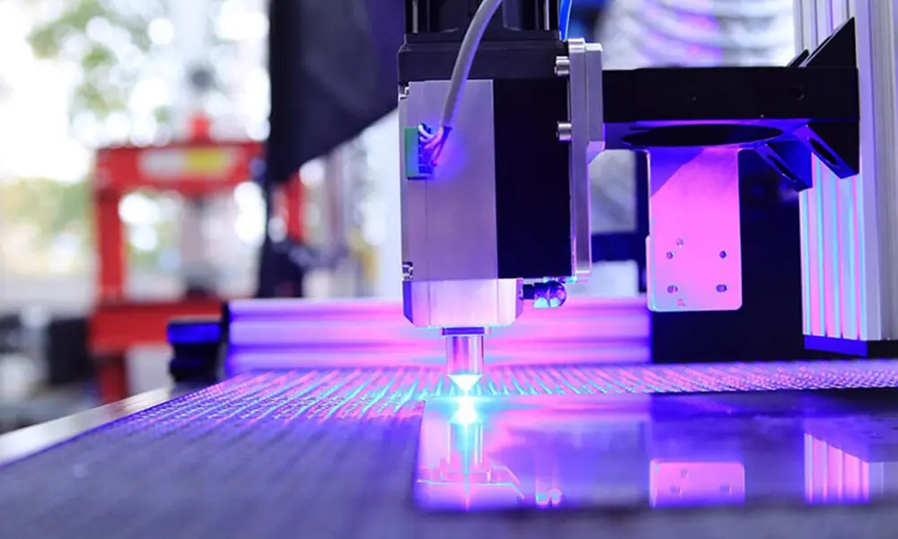
リフローはんだ付けガイド:工程、プロファイル、不具合
リフローはんだ付けとは、ステンシル印刷したはんだペーストを加熱して溶かし、表面実装部品の端子になじませてから冷却し、接合部を形成することで、部品をプリント基板に取り付ける工程です。ほぼすべての現代的な電子製品で中心となる組み立て方法であり、最も高くつくミスが発生しやすい工程でもあります。…
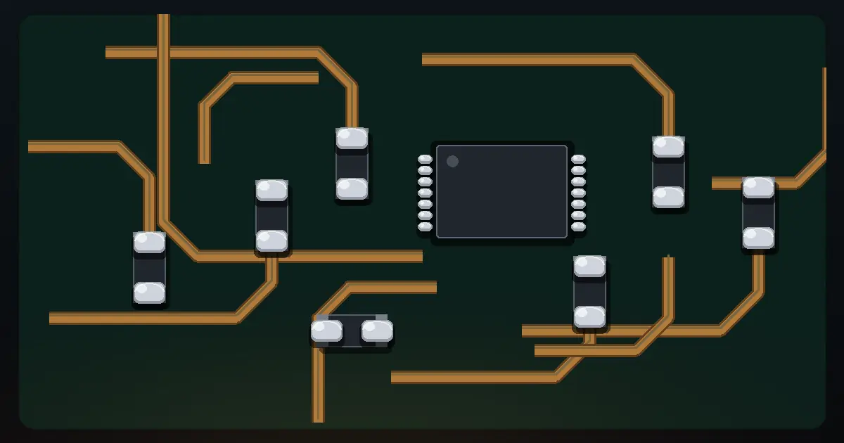
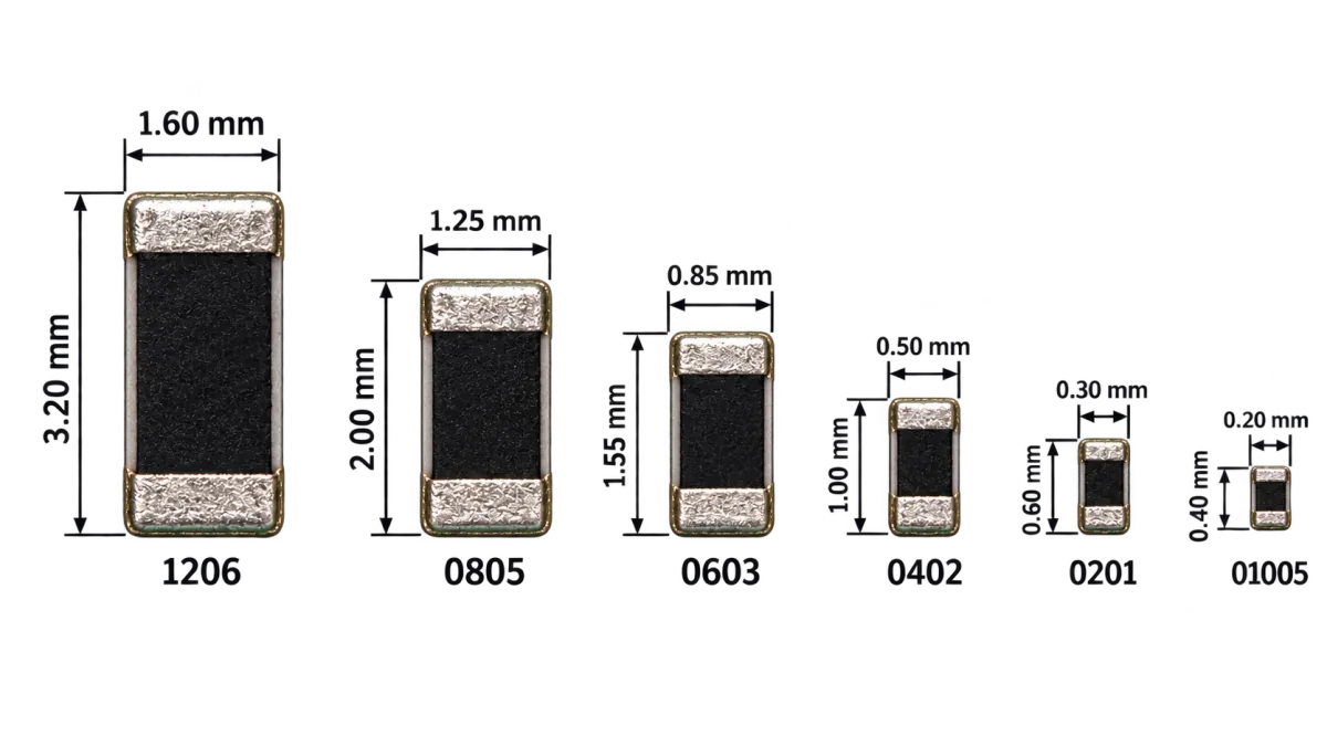
SMD抵抗器ガイド:コード、サイズ、フットプリント、定格
SMD抵抗器は、リードのない長方形のパッケージに収められた固定抵抗器で、プリント基板の穴に通すのではなく、基板表面のランドにはんだ付けします。一般に、基板上で最も数が多く、データシートではなく慣例に基づいて指定されることが最も多い部品です。多くのガイドでは…
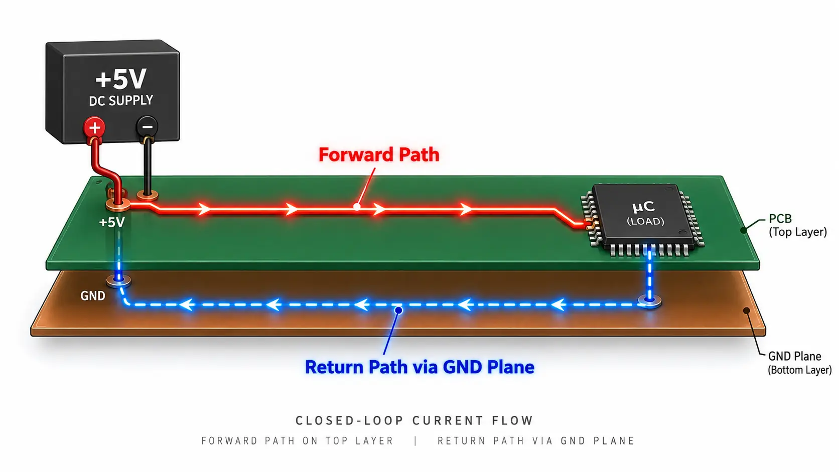
GNDとは?意味、種類、PCBのグラウンディングを解説
GND appears on almost every circuit diagram, PCB, power supply, and electronic module. It is often described as “zero volts” or “the negative terminal,” but neither description is universally correct. In electronics, GND stands for ground. It is the reference node against which other voltages are measured and, in many circuits, part of the path…
スルーホールとは?PCBの種類、用途、設計ガイド
A through hole is an opening that passes completely from one side of a printed circuit board (PCB) to the other. It may be plated with conductive copper to create an electrical connection, or left unplated for mechanical use. Through holes are commonly used for component leads, connectors, vias, mounting hardware, alignment pins, and slots.…

LEDのアノードとカソード:正極端子と負極端子の見分け方
An LED (Light Emitting Diode) is a polarized semiconductor device that allows current to flow in only one direction. To illuminate an LED, you must connect its positive and negative terminals correctly within your circuit. On standard through-hole LEDs, the longer leg and the rounded side represent the anode, while the shorter leg and the…

0402抵抗器ガイド:サイズ、仕様、選び方
Hardware design always comes down to a battle for board space. As consumer wearables, IoT devices, and high-performance computing modules pack more features into smaller enclosures, printed circuit board (PCB) real estate has become an incredibly valuable commodity. Moving away from legacy through-hole parts and bulkier surface-mount devices (SMDs) is no longer optional—it is a…
IPC-TM-650を解説:PCB試験方法、主要手順、品質管理での活用
“Test to IPC” is not a complete PCB requirement. A supplier still needs the method, revision, samples, conditions, and acceptance criteria before it can quote or run the work. IPC-TM-650 is the procedure side of PCB testing. It helps engineers choose a way to measure a board characteristic. The governing specification, drawing, or contract still…

PCBラミネート選定のためのFR-4材料特性
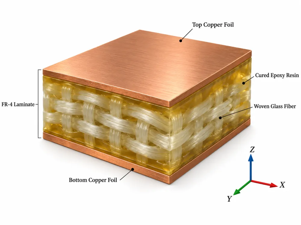
The FR-4 material properties that matter most depend on what your PCB must withstand: electrical signals, assembly heat, operating temperatures, voltage stress, moisture, and mechanical loading. Start with dielectric constant and loss, thermal expansion and stability, insulation performance, and mechanical requirements. FR-4 is a flame-retardant, glass-reinforced epoxy material class. It does not identify one fixed…
PCBビアガイド:種類、設計ルール、選び方のヒント
A PCB via is a plated interconnect that lets signals, power, ground, or heat move between copper layers in a printed circuit board. Via choice affects routing density, fabrication cost, assembly yield, signal integrity, and thermal performance, so it should be part of stackup and DFM planning, not a cleanup step at the end. For…

パワーPCBと電源PCBの設計ガイド
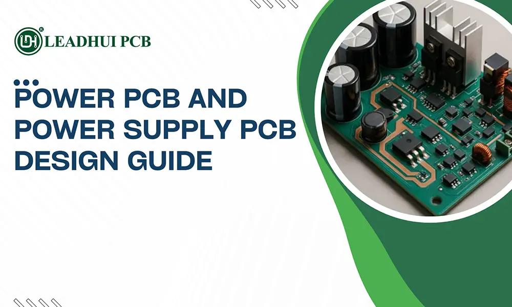
A power PCB is the circuit board that receives, converts, regulates, distributes, or monitors electrical power. A power supply PCB is a more specific type of power PCB that converts an input source—such as AC mains, a battery, USB power, or a DC bus—into stable output voltage rails for an electronic product. The quality of…
SMTとは:表面実装技術をわかりやすく解説
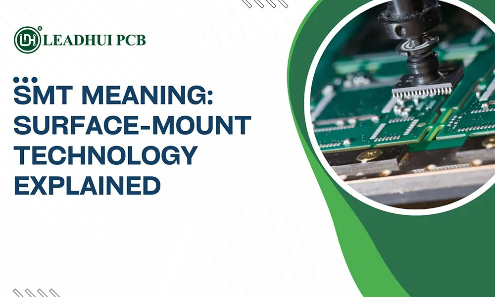
SMT means Surface-Mount Technology: a method of attaching electronic components directly onto the surface of a printed circuit board (PCB). Rather than inserting long component leads through drilled holes, SMT uses small surface-mount components that are placed on solder-coated pads and permanently connected through controlled heating. In practical terms, SMT is what makes modern electronics…
Dual Inline Package Meaning: Pinout, Dimensions & Assembly Guide
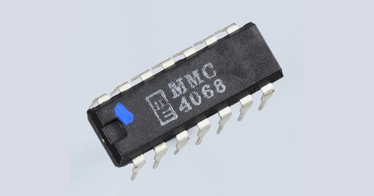
A dual inline package (DIP) is a component package with two parallel rows of leads. Many DIPs are inserted into holes in a circuit board or a socket. The package describes the part's physical form; it does not tell you what the circuit inside does. For a board designer, identifying a DIP is only the…